Article

CO2 Laser Manufacturing of Miniaturised Lenses for Lab-on-a-Chip Systems

by
Mazher-Iqbal Mohammed
* and
Marc Phillipe Yves Desmulliez
Earl Mountbatten Building, School of Engineering & Physical Sciences, Research Institute of Sensors, Signals and Systems, MicroSystems Engineering Centre (MISEC), Heriot-Watt University, Edinburgh EH14 4AS, Scotland, UK
*
Author to whom correspondence should be addressed.
Micromachines 2014, 5(3), 457-471; https://doi.org/10.3390/mi5030457
Submission received: 30 May 2014 / Revised: 11 July 2014 / Accepted: 15 July 2014 / Published: 21 July 2014
(This article belongs to the Special Issue Microlenses)

Abstract

:
This article describes the manufacturing and characterisation of plano-convex miniaturised lenses using a CO2 laser engraving process in PMMA substrates. The technique allows for lenses to be fabricated rapidly and in a reproducible manner at depths of over 200 μm and for lens diameters of more than 3 mm. Experimental characterisation of the lens focal lengths shows good correlation with theory. The plano-convex lenses have been successfully embedded into capillary microfluidic systems alongside planar microlenses, allowing for a significant reduction of ancillary optics without a loss of detection sensitivity when performing fluorescence measurements. Such technology provides a significant step forward towards the portability of fluorescence- or luminescence-based systems for biological/chemical analysis.

Graphical Abstract

1. Introduction

Lab-on-a-chip technologies have revolutionised biological- and chemical-based processes for diagnostics-based applications. In particular, optical-based interrogation techniques have become the most prevalent means of end-point quantification. Such techniques are, however, typically performed using bulky assisting instrumentation, thereby negating the advantages of device miniaturisation [1,2]. An elegant approach to remedy this bottleneck with respect to true device portability and miniaturisation includes the use of embedded on chip microlenses and microlens arrays [3,4,5,6,7,8,9,10] for not only lab-on-a-chip systems, but also for alternative applications, ranging from optical storage/communications, high definition displays to a host of biomedical instrumentation [11].
Various microlenses and microarray structures have been fabricated in a range of substrates using techniques, such as photolithography/reactive ion etching [3,4,5,6,7], surface tension-based curing [10,11], laser ablation, engraving and thermal expansion [8,9,12,13,14], thermal reflow [15,16], embossing [17,18] and inkjetting [19,20]. Of these fabrication processes, CO2 laser engraving is an attractive alternative to established micro-manufacturing techniques for the production of optical components, and such a technology has a rapid turnaround time and does not require fixed photomasks, embossing tools or a clean room environment and is suited to polymer manufacturing, a substrate most commonly used for the fabrication of various microsystems [8,9,21,22,23,24,25]. However, without adequate post-processing, the quality of manufactured microfluidics and the surface quality of the lenses are poor compared to techniques, such as photolithography or thermal reflow.
This article describes a manufacturing process whereby plano-convex lens structures are formed by CO2 laser etching of poly(methyl methacrylate) (PMMA) polymer surfaces, using a graded power function with raster scanning. The resulting lens structures are then polished to a high degree of clarity using simple, backend processing of the lens surface, comprising abrasive hand sanding and polishing with rubbing compounds, followed by thermal annealing. The final lens structures can be fabricated with a high degree of reproducibility, rapidly and with the versatility to readily alter the physical parameters of the lens, providing considerable scope for tailoring of the focal lengths of the lens. CO2 laser systems have been used previously to form planar lens structures [8,9] and lens structures upon optical fibres [14]. However, this is the first such demonstration of the CO2 laser engraving using a graded power function by which to produce both single and arrays of plano-convex lenses in a bulk polymer material. Additionally, we demonstrate how both 2D planar and 3D plano-convex lenses can be readily integrated into microfluidics-based systems, providing a usable lab-on-a-chip platform for a range of optical-based test inspection and biological/chemical-based reaction end-point quantification.

2. Experimental Section

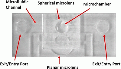
2.1. Materials and Fabrication

All microlens and microfluidic structures demonstrated in this work were manufactured using a Class 2 CO2 laser etching system (Helix 24, Epilog, Golden, CO, USA), which operates at a maximum power of 40 W, a maximum scan speed of 96 mm s−1, a wavelength of 10.6 μm with a spot size of 76–127 μm. All devices were manufactured from CLAREX® precision thin sheet PMMA, made by a specialist cell-casting technique, which ensures very high surface uniformity, and was purchased precast from Weatherall Equipment & Instruments Ltd (Bucks, UK). Designs of the plano-convex lenses were created using Corel Draw X4 (Corel Software, Ottawa, ON, Canada) interfaced directly with the CO2 laser.
Within the Epilog system, the CO2 laser is mounted in the device, such that its focal point is directed into reflecting and focusing optical elements, which translate the beam in the x- and y-directions through the use of two stepper motors. Samples to be processed are brought into focus with the laser upon a working stage, which is translatable in the z-direction. PMMA is processed based on its ability to absorb the radiation produced by the laser, with the power required to etch a given thickness depending on the melting and vaporisation temperatures of the polymer. The laser power and scan speed can be adjusted across a percentage scale in 1% increments, across either vector or raster power modes, as described in previous articles [21,22].
For the final manufacturing phase, the devices were constructed from a double-layer PMMA laminate, with the microfluidic channels and 2D lenses on the lower 1 mm-thick layer and plano-convex lenses on the upper layer. The upper layer also acts as a seal for the microfluidic channels and provides entry and exit ports for the test fluid, with flow being initiated and maintained through capillary action. Microchannels were fabricated in a single pass using a laser scan speed of 35% and power of 30%, with the laser set to low power raster mode, creating microchannels approximately 300 μm in depth. 2D lenses were created in a single pass of the laser with a scan speed of 30% and power of 80%, with the laser set to the high power vector mode to cut through the PMMA substrate, creating a 2D lens structure with a thickness equal to that of the substrate. The 2D lenses were singulated from the substrate to ease the polishing of the surfaces. They were also cut into a squared section of PMMA, such that they can be slotted back into the chip containing the channels for the subsequent bonding process. The polishing of the 2D lens surfaces is performed in an identical fashion to the plano-convex lenses, as described in Section 2.2.
The devices were bonded using a thermal compressive bonding procedure, described in [21]. The entire bonding procedure can be completed within approximately 2–3 h and leads to a permanent bonding of the PMMA through the controlled melting and re-solidification of the surfaces of the two PMMA layers. Briefly, the two laminate layers were covered with borosilicate glass microscope slides over the top and bottom layers and then placed between two 10 mm-thick steel plates and compressed together. The plates were then placed into a convection oven and heated under a slow thermal gradient (2–3 °C min−1) above the glass transition temperature of the PMMA (170 °C), for a period of approximately 40 min. Following this, the oven is cooled to 80 °C and held for duration of 30 min before being cooled to room temperature.

2.2. Plano-Convex Lens Modelling and Fabrication

In addition to the unique manufacturing process that makes use of the graded power function of the laser engraving system, the 3D plano-convex lenses in this work yield several distinct advantages compared to the use of our previously demonstrated 2D lens structures. Firstly, the 2D lenses only allow for light to be directed within the plane of the chip, and the 3D lenses allow for light to be collected, or directed, orthogonal to the chip plane, making both lenses suitable for distinctly different applications. Therefore, collecting emission light orthogonal to the chip plane removes the cross-talk from excitation and emission light, thereby maximising the detection signal. For orthogonal chip light emission detection, the 2D lenses are not suitable. However, the 3D plano-convex lenses readily allow for this orientation, and their fabrication within the bulk chip substrate layer means that they can easily be integrated into the laminate chip bonding method used in this work. Additionally, the 3D lenses provide a greater collection efficiency of light, allowing for a near 2π collection angle, whereas collection with 2D lenses approximately has a collection angle of π. Ultimately, this makes the 2D lens structures ideal for excitation purposes, where light generally needs to be delivered in the chip plane, and the 3D plano-convex lenses are suited for emission collection optics.
In our previous work, we have demonstrated the CO2 laser operating with either power on or off [8,
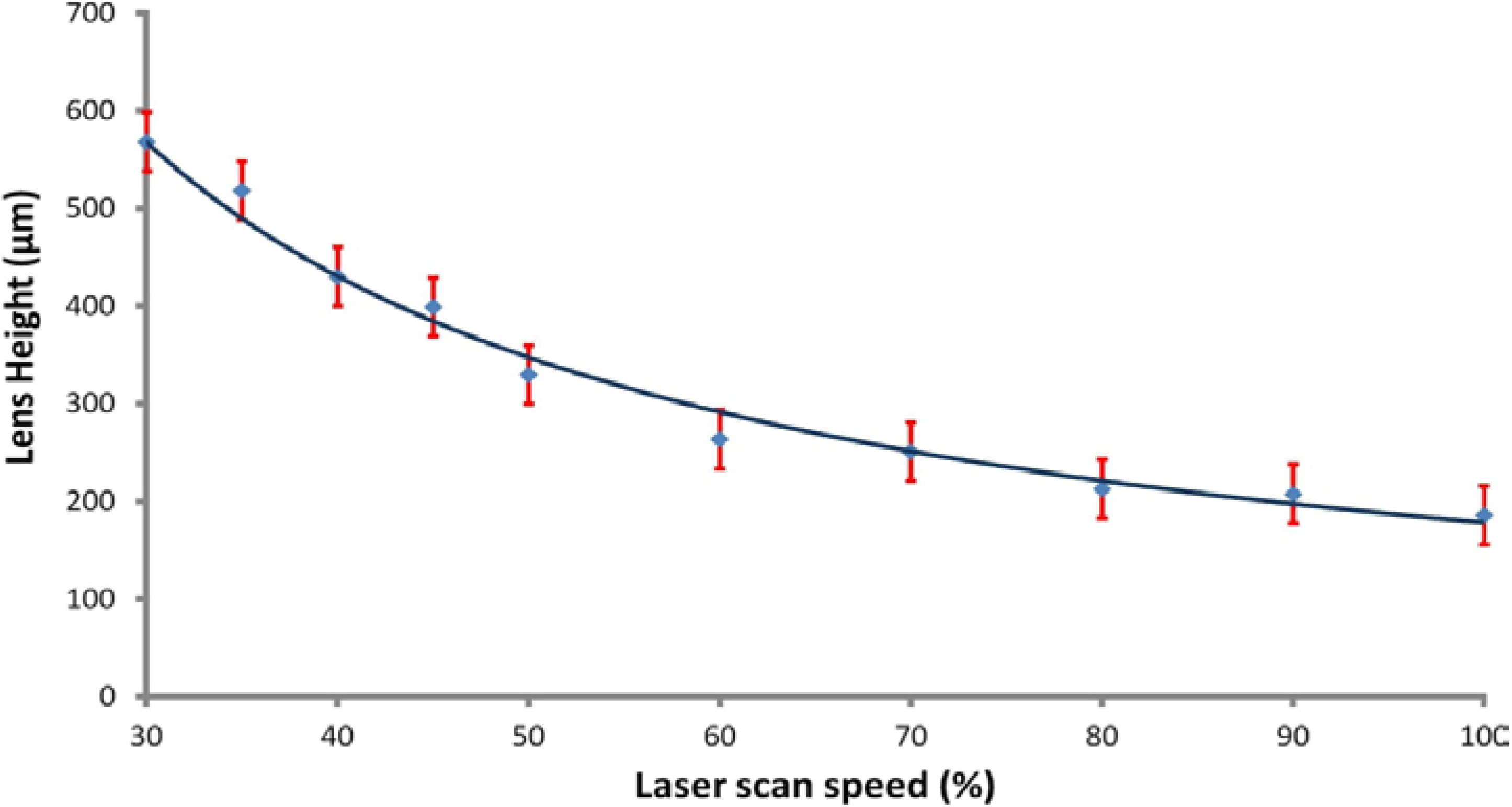
21]. In this work, the laser was used in an analogue fashion to yield greater functionality during fabrication to create the 3D features. In that regard, a circular design, which comprises the plano-convex lens, was superimposed upon a rectangular area. The rectangular area is removed by direct etching using the laser system. The use of the rectangular area surrounding the lens is required to allow space for polishing of the lens surface post engraving. The power distribution of the laser was graded from full power at the rectangle area and circle edges and gradually moving to zero power at the centre of the circle. This resulted in the creation of a plano-convex lens in the centre of the rectangular etched area within the PMMA. The curvature of the lens can be adjusted depending upon the radius of the circle design and by control of the depth of etching in the low power, raster scan mode of the laser. Using the CO2 laser at maximum power in raster scan mode, Figure 1 illustrates the attained average lens depth of etch as a function of the laser scan speed for a 5-mm diameter lens fabricated into a 2 mm-thick PMMA substrate. Tests were also performed using multiple passes of the laser over a single target area, allowing for the maximum depth of etch to be extended beyond that of a single pass. During the subsequent passes, the laser spot is out of focus and imparts less power onto the target area. This has the effect of partially “cleaning” residual, condensed PMMA material. For this work, 2 passes were performed with the power set to maximum and with speeds of 45% and 60% for the first and second pass, respectively. This produced a lens structure with an approximate depth of 600 ± 30 μm, which was used as a standard depth to investigate various diameter lens structures.
Figure 1. Ablation depth as a function of laser scan speed for maximum raster mode laser power.
Micromachines 05 00457 g001
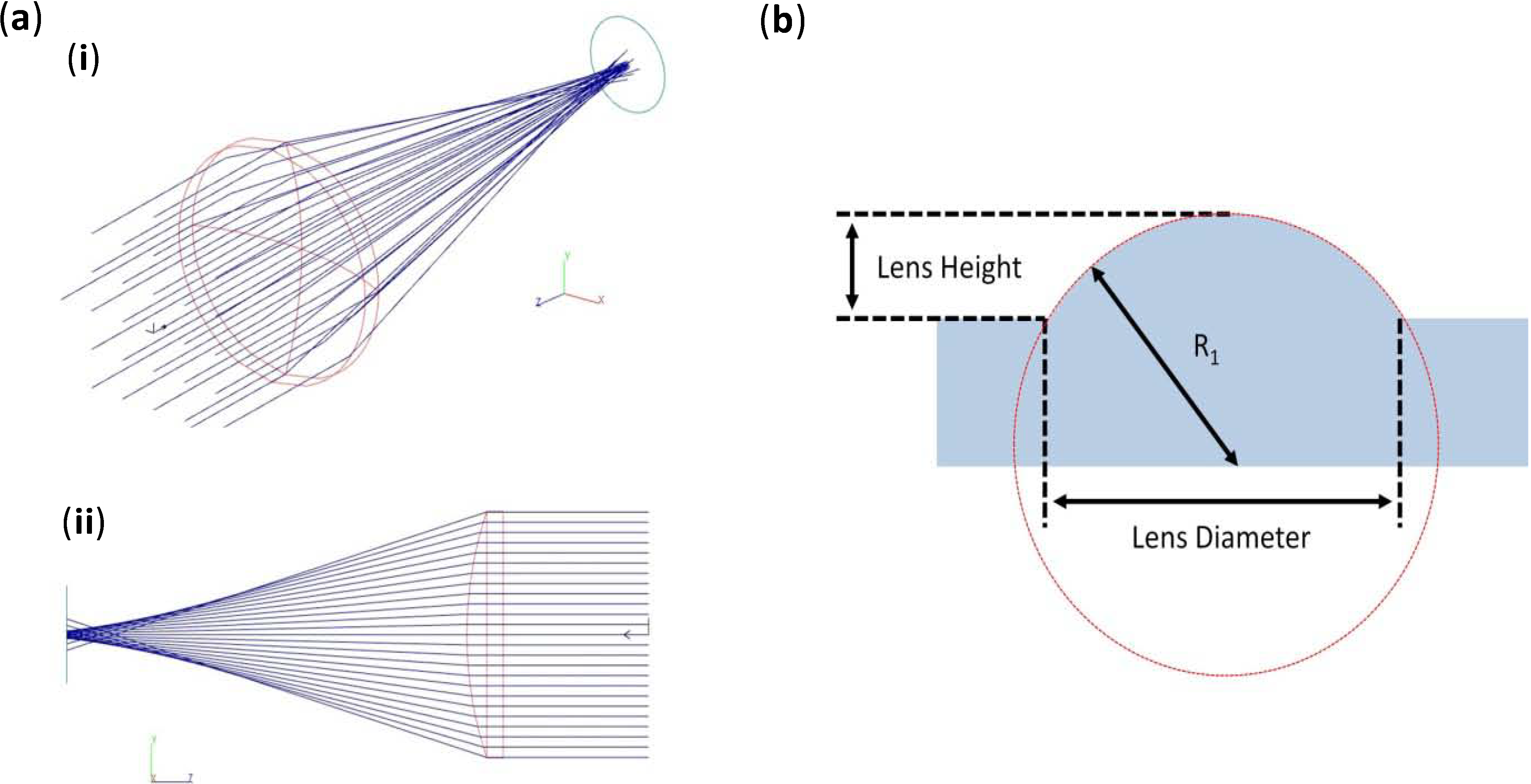
Optical simulations were performed using OptiCAD 7.0 (OptiCAD Corporation, Santa Fe, NM, USA) modelling the focusing of light from a collimated white light source through a plano-convex spherical lens and onto a virtual detection area. This model mimics our experimental set-up allowing for the determination of the focal length of the lens. In all simulations, a refractive index for PMMA of 1.49 was used. Figure 2 shows ray path simulations for a 5 mm-diameter plano-convex lens. Several lens diameters were examined, and a summary of the lens properties and predicted focal distances can be found in Table 1. The simulations revealed the spherical aberrations that would be present in such a lens design, which results in a range over which the true focal distance of the lens will be found, and this range is expressed in Table 1.
Figure 2. (a) Simulated results of the focusing of a collimated light source through a 5-mm plano-convex lens showing (i) 3D and (ii) a plan view of the lens and light rays; (b) A diagram illustrating the parameters of the fabricated lenses within a PMMA bulk substrate, as stated in Table 1.
Micromachines 05 00457 g002
Table 1. Theoretical results for various lens diameters and their respective focal lengths. R1 is defined in Figure 2.
Lens diameter (mm)Lens height (mm)R1 (mm)Simulated focal range (mm)
0.250.612.50.19–0.21
0.50.60.250.44–0.46
10.60.50.92–0.95
30.62.354.2–4.3
50.6611.2–11.5
The plano-convex lenses were fabricated in a similar fashion to PMMA-based laser-ablated 2D lenses [
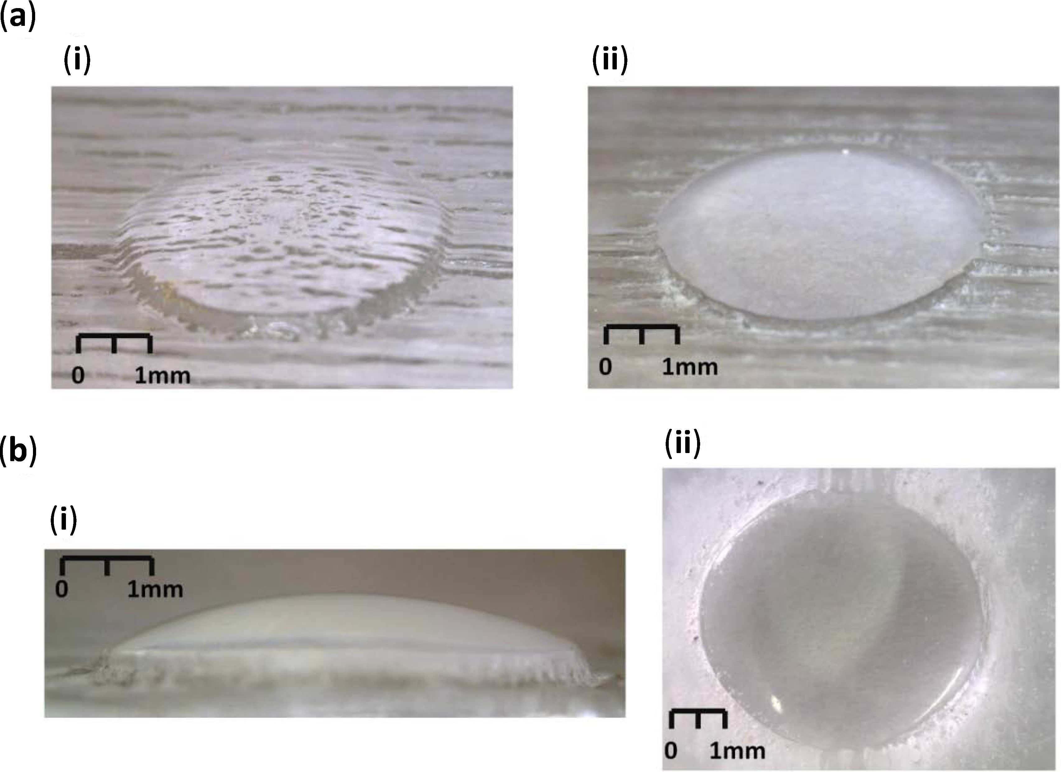
8]. The surfaces of the lenses were found to be rough, due to the nature of the thermal vaporisation and condensation process, as observed in Figure 3a-i. Following the initial laser etching, the lenses were then polished manually by hand, by firstly sequentially sanding using 60, 240, 600, 1200, 2400 and 4000 grit wet and dry sandpaper to remove major defects. Lenses were sanded by placing a 1 cm2 piece of wetted sand paper over the lens, applying light pressure with the index finger and rotating the paper in a clockwise circular manner, with the whole procedure taking approximately 5–6 min. This was followed by a two-stage hand polishing with an acrylic polymer cutting compound (Glass Polish Ltd., Tolworth, UK) to remove the majority of remaining abrasions and scratches, with this procedure taking approximately 5 min. Following polishing, the lenses underwent a final stage of thermal processing, whereby the substrate is heated above the glass transition temperature of the PMMA for 30 min, resulting in the liquefaction of the lens surface. At this stage, the surface tension effects during liquefaction remove any remaining minor defects, resulting in a high quality finish to the lens surface, as can be seen in Figure 3a-ii,b. The process of defect removal had measured effects on the radius and height, and each was quantified by taking the average across 10 independently manufactured 5 mm-diameter lenses. The radiuses of the lenses were found to contain negligible differences, with an average reduction of 5–10 μm over the 5 mm of diameter. The height at the centre of the lens relative to the original substrate height was found to be reduced by approximately 250 ± 20 μm. These changes were factored into the optical simulations to reflect the true geometry of the manufactured lenses.
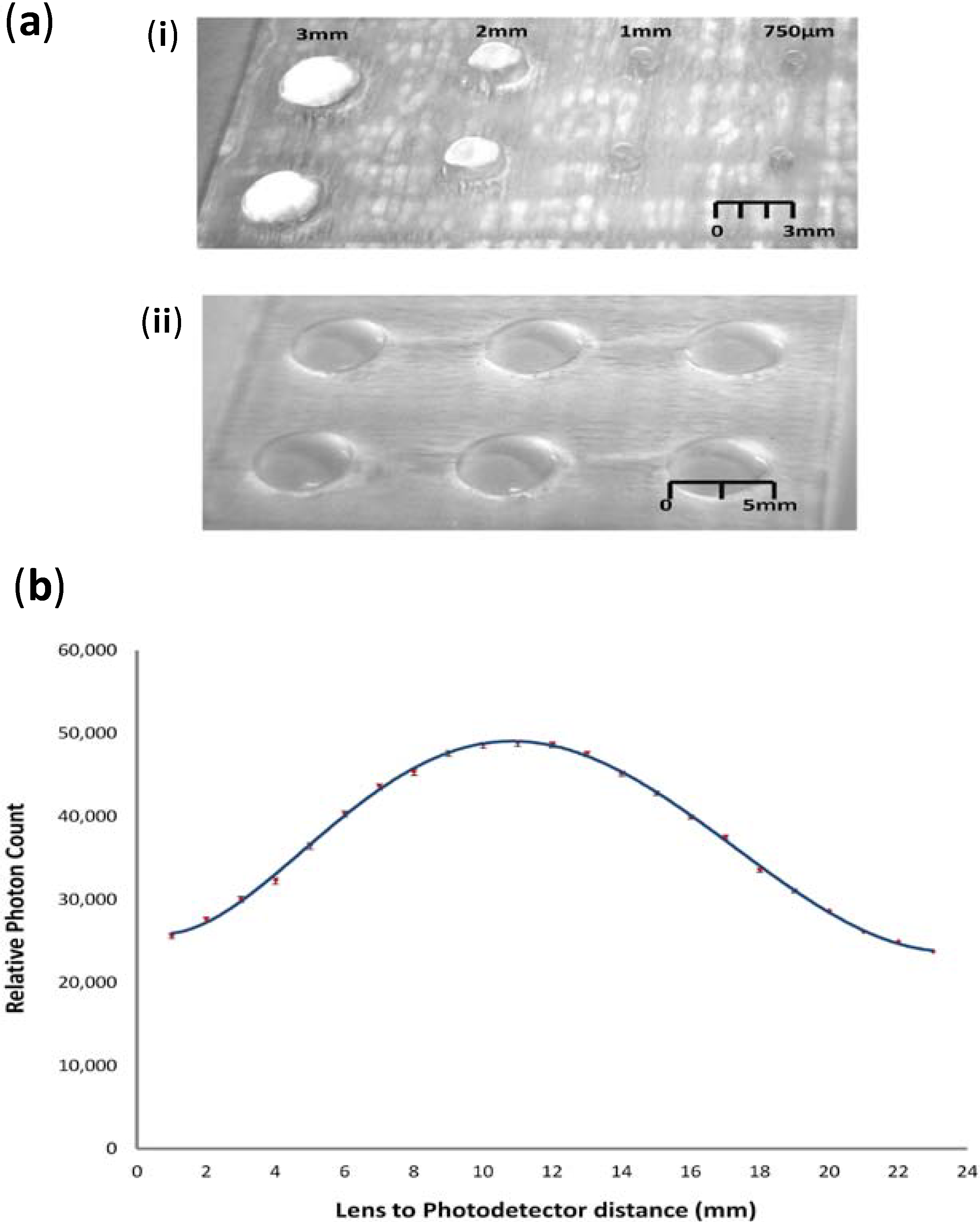
The graded spatial thermal processing of the PMMA substrate was examined over varying lens diameters to determine the limitations to the geometry of the manufactured lenses. The CO2 laser system has a minimum manufacturing resolution of approximately 100–150 μm. The smallest manufacturable size is likely to be significantly larger for the laser stepper motor to create the lens curvature upon the PMMA surface. Various-sized lenses were manufactured with diameters of 5 mm, 3 mm, 2 mm, 1 mm and 750 μm, and the quality of the final structures was assessed to determine the limitations of the proposed manufacturing process, as described later in the article. It was determined that the 5 mm-larger diameter lens structure was likely to be the most practical for implementation into a working device, given its focal length and the need to manually align the photodetector with the chip system. Therefore, work was focused primarily on the characterisation of this type of lens.
Figure 3. (a) Photographs of a 5 mm, spherical PMMA lens (i) post-laser ablation and (ii) post-polishing and thermal annealing; (b) The same PMMA post-polished and thermally annealed lens in (i) side profile and (ii) overhead profile.
Micromachines 05 00457 g003

2.3. Fluorescence and Light Detection

The manufactured lenses were validated through the detection of both light from various LED sources and from the emission of excited fluorophores placed into microfluidic systems. For all characterisation-based experiments, detection was achieved using a USB-based spectrometer (USB2000+, Ocean Optics, Dunedin, FL, USA) in conjunction with a 200-μm coupling optical fibre (Numerical Aperture (NA) = 0.22) mounted upon an x-y-z translational stage. Focal length determinations were achieved using a blue collimated LED source (M470L3-C1, Thorlabs, Ely, UK) and the diameter of the light column controlled by an in-house build optical aperture. A schematic of the experimental setup can be seen in Figure 4a.
For testing in the microfluidic system, serial dilutions of fluorescein isothiocyanate (FITC) dye (λExcitation = 494 nm and λEmission = 518 nm) were used as a demonstrator for fluorescence detection. In this work, a 1-nM FITC solution was used for all testing of lens properties. This was made fresh in a stock solution combined on the first instance with ethanol, following the manufacturer’s recommendations, and then subsequently diluted with deionised water. As ethanol degrades PMMA, which was used as the vessel for FITC, a water-based dilution methodology was used to preserve the integrity of the microfluidic channels. Excitation of the fluorophores was achieved using a 3-mm Nichia ultra-bright blue LED (NSPB300A, RS Components, Glasgow, UK) and a band pass excitation filter (FB490-10, Thorlabs, UK) with λTrans = 490 ± 5 nm (approximately 48% transmission), both mounted into a custom-built holder cradle. Fluorescence detection measurement was achieved using a H9858 photosensor module (Hamamatsu, Welwyn Garden City, UK), in conjunction with an FITC-optimised band pass emission filter (HQ535-50m, Chroma, Bellows Falls, VT, USA), λTrans = 535 ± 25 nm (approximately 75%–80% transmission). A schematic of the experimental set up can be seen in 
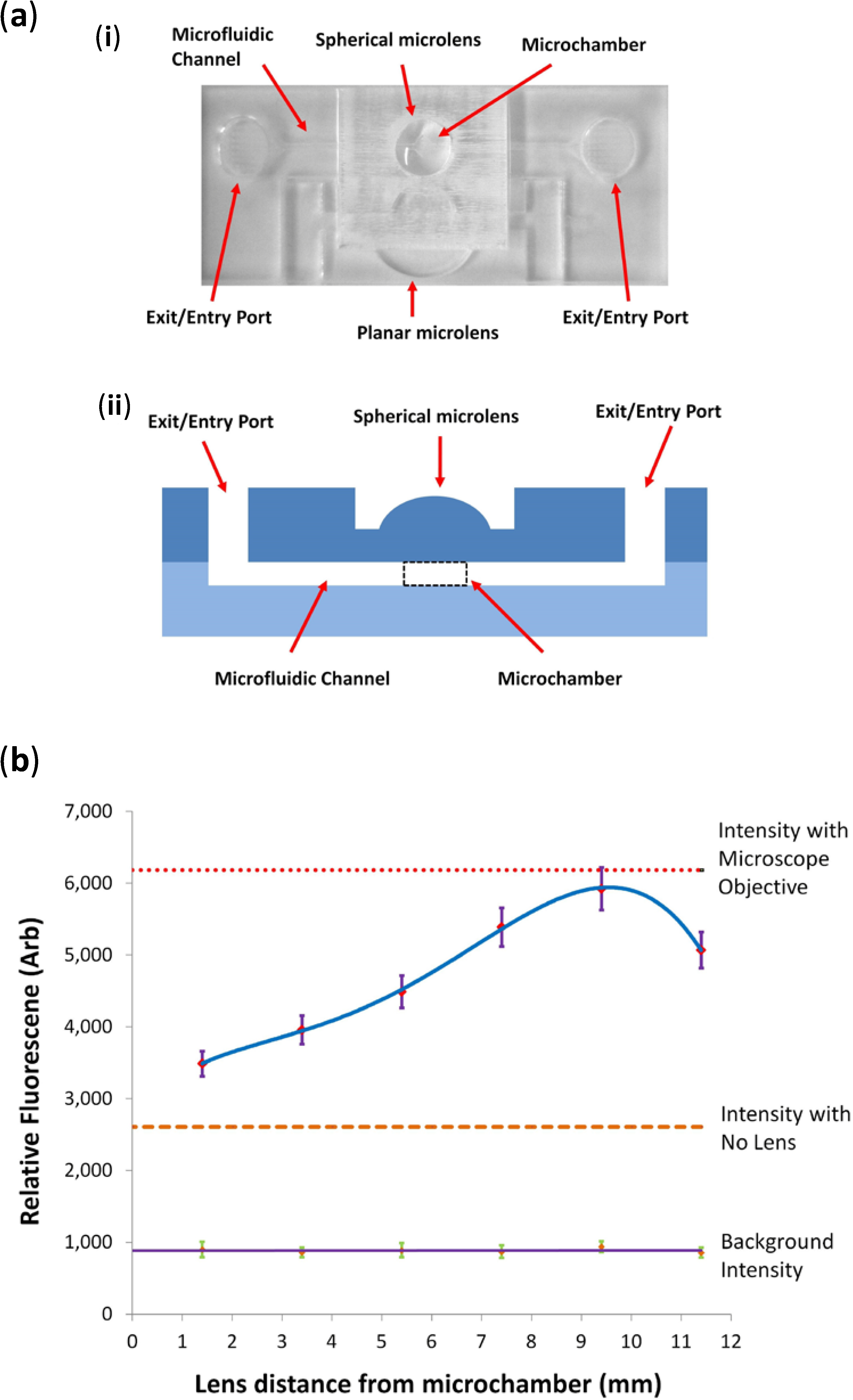
Figure 4b. The photodetector and emission filter were both housed within a custom-built cradle, to preserve the alignment of the two components and to reduce background light from entering the active area of the detector. A secondary rig was built to house the excitation LED/emission filter and to create a cradle into which the chip could be placed, such that its final orientation would leave the 2D planar lens and microchamber of the fluidic chip in direct alignment with the LED and photodetector, respectively. The photomultiplier module, LED and filters were set up in a configuration as illustrated in Figure 5b, and the photodetector was mounted a distance of 40 mm above the bottom of the chip holding cradle. As a benchmark comparison, fluorescence measurements were performed using a 10× microscope objective (Thorlabs, UK) as the light collection optics, placed approximately 500 μm above the fluidic microchamber, in a configuration described previously [8]. Such a system has been demonstrated previously by our group to provide FITC detection limits of 10 fM, which is comparable to the detection capabilities of commercial fluorescence reader systems. The use of this benchmark setup allows us to examine the efficiency of the optical component only, as we shall keep the excitation and detection apparatus the same. This therefore eliminates the variability from factors, such as detector sensitivity and excitation power emission, that have a different fluorescence setup being used, thereby providing a more fair comparison of the devised plano-convex lenses against commercial-grade optics.
Figure 4. Schematic of the experimental setup to determine (a) the lens focal length and (b) the FITC fluorescence intensity measurements.
Micromachines 05 00457 g004

3. Results

3.1. Manufacturing Limitations and Characterisation

Investigations were initially performed to validate the smallest repeatable lens size that could be manufactured by the proposed fabrication process. Figure 5a shows images of several lens structures ranging from 3 mm to 750 μm in a single array. The defect removal procedure was focused on the lenses only and not on the bulk of the PMMA substrate material, which had been engraved away using the CO2 laser. The ability to use a manual polishing methodology was constrained by the size of the lens structure and the ability to physically feel the surface of the lens during hand sanding. Additionally, the qualitative nature of the process limits the roundness precision of the lenses, which were found to suffer a discrepancy between what could be achieved and the desired lens curvature. Errors in precision were quantified to be on average a minimum of 1–2 μm and a maximum of 30–40 μm above or below the intended curvature respectively. This discrepancy was found to be uniform across the various lens diameters from the average measurement of several lens surfaces under a microscope and has the influence of increasing the spherical aberrations. As the discrepancy in the roundness was found to be uniform, their influence is most pronounced for smaller lens diameters, negatively impacting the ability to achieve a tight focus of a light source or to produce a sharp image when used for magnification purposes. Through qualitative testing, for lens diameters of over 3 mm, the influence on achieving a tight focus from a light source or producing a sharp image of a magnified test structure was found to be negligible. Despite the demonstrated qualitative adequacy of the hand sanding/polishing method, it would be desirable to standardize the polishing procedure through the automated use of an industrial, sanding, lapping and polishing device. These devices could potentially provide more uniform pressure and sanding/polishing action across the surface of the lens, improving the roundness of the lenses and, thereby, reducing spherical aberrations. Tests were also performed to use the Epilog laser system to polish the surface of the manufactured lenses using a methodology described previously [26], but attempts were unsuccessful at adequately removing defects. Given greater control of the laser parameters (raster speed, power, etc.), the current CO2 laser could potentially be used to polish the surface of the lenses. We aim to investigate the feasibility of such measures in future work.
For diameters of less than 750 μm, the laser was incapable of forming the desired lens structure in a reproducible manner, due to limitations in the resolution of the x-y translation stage of the Epilog equipment. It was therefore concluded that the smallest repeatable diameter of lens manufacturable by the described process was above 3 mm.
Figure 5. (a) Photographs of spherical PMMA lenses (i) of sizes of 3 mm, 2 mm, 1 mm and 750 um; and (ii) a 5 mm lens array, post-polishing and thermal annealing; (b) Results for the average focal length determination of several 5 mm-diameter spherical lenses.
Micromachines 05 00457 g005
Given the greater level of repeatability of larger diameter lens structures, the remainder of this work focused on the characterisation of the 5 mm-diameter plano-convex lenses. Each lens was characterised using the experimental setup illustrated in Figure 4a, whereby an optical fibre, 200 μm in diameter (0.22 NA ≈ 25° full angle of acceptance), connected to a photodetector, was placed at the midpoint of the lens and ,using a translational stage, was moved progressively away from the lens in 1 mm increments. Light was then shone from a collimated LED source, through a lens, where it was focused into the direct path of the optical fibre. It was believed that, given the limited acceptance angle, as the fibre was moved closer to the focal point of the lens, the intensity measured by the photodetector would increase. Conversely, as the fibre moves away from the focal point, the intensity would also decrease. Results for the average over five lenses are illustrated in Figure 5b, were a focal point of approximately 10.9 mm was determined from extrapolation of a line of best fit. This result is in good agreement with the predicted result of 11.2–11.5 mm, with any discrepancies being explained by the minor variations in the lens height and the alignment of the optical fibre during experimentation.
It was possible given the agile nature of the laser engraving process that lens arrays could be produced and applied to the multiplex focusing of multiple sources, such as those found in multiplate well systems. Figure 5a-ii shows a picture of a 5 mm-diameter lens array, fabricated with a spacing of 5 mm from each edge of the lens structure.

3.2. Microfluidic Chip Integration

The rapid prototype manufacturing process was investigated to integrate the plano-convex lens directly into a microfluidic chip design, in a similar fashion as the integration of 2D planar lenses achieved by our group in previous works [8,9]. The aim of such a device would be to operate as an integrated excitation and detection platform for fluidic and solid phase-based biological and chemical processes, such as fluorescence/luminescent DNA- [27,28] and protein- [8,9,29,30] based reactions. Such a design would provide a lab-on-a chip solution that completely eliminates complementary, off-chip optical elements. As our aim in this work is to focus on aspects pertaining to micro-optical systems integration, we shall not elaborate on the dynamics of the fluidics components, which we have characterised previously [22].
Figure 6a illustrates the complete microfluidic chip design, with the lower laminate layer containing the microfluidic channel, micro-chamber and 2D planar lenses and the upper layer containing the entry/exit ports and the plano-convex lens. The chip had approximate dimensions of 60 mm × 25 mm × 3 mm. For visualisation of all the chip components, the bulk engraved area surrounding the plano-convex lens has been left intact. Prior to a measurement, this area is covered with a layer of blackened masking tape, leaving only the lens exposed, in order to remove any unwanted scattering of the excitation and emission light on the roughened surface from entering the active area of the photodetector, thereby improving detection sensitivity. For experimentation, one of the ports was loaded with 20 μL of the 1 nM FITC dye, which migrated to fill the fluidic system through capillary forces. Following loading of the test dye, the microfluidic chip was placed into the cradle of the custom-built excitation and fluorescence reader, and the emitted fluorescence was measured.
Figure 6. (a) (i) Photograph of the complete microfluidic chip with integrated planar and spherical lenses and (ii) annotated schematic of the microchip cross section; (b) Detected fluorescence intensity from a 1-nM sample of FITC within the chip as a function of the distance of the lens from the micro-chamber. As a comparison, results are shown for systems with no spherical lens and additional collection optics; and no spherical lens and a 10× microscope objective for emission collection.
Micromachines 05 00457 g006
Initial tests were performed on a fluidic chip with the 600-μm depth, 5 mm-diameter plano-convex microlens engraved into a 2-mm substrate, placing the lens at a distance of approximately 1.4 mm from the upper surface of the FITC loaded micro-chamber. Following this measurement, additional microfluidic chips were fabricated to include the 2D planar lens and a blank 1 mm-thick upper sealing layer, with only entry and exit ports. This allowed for a plano-convex lens engraved substrate and spacers to be placed upon the chip surface to examine the change in measured fluorescence with increased separation distance. To increase the separation distance, various 1 mm-thick PMMA substrates, of equal size to the chip, were placed in between the unmodified upper layer chip and a PMMA layer containing the plano-convex microlens. Results of the fluorescence detection can be seen in Figure 6b, where it was found that the use of the lens significantly increased the detected fluorescence emission in comparison to when no lens was placed on the chip. The largest increase in detected fluorescence was achieved for a separation distance of approximately 9.4 mm, which provided an increase in fluorescence signal by approximately a factor of 2–2.5. Examining the results against the measurement using the collection optics benchmark, it was found that the maximum intensity achieved using the plano-convex lens system was comparable to the use of the microscope objective, as can be seen in Figure 6b. The lenses were significantly smaller in dimensions, being a height of 600 μm and a radius of 5 mm, compared to a height of 50 mm and maximum radius of 30 mm for the microscope objective. It is the aim of future work to develop the system further to reduce the separation distance of the lens to the microchannel by means of altered single lens geometry or the use of a compound multi-lens system. However, even with the added height of the separation distance, the 10 mm total height of the system compares favourably to the microscope objective benchmark. This, in addition to the integration of the lenses, provides significant advantages of the demonstrated system in terms of overall device portability, a bottleneck still to be fully addressed in current lab-on-a-chip and microfluidic systems.

4. Conclusions

In this paper, we have reported the creation of plano-convex microlens structures within PMMA substrates by means of 3D CO2 laser engraving. The lenses can be made rapidly and in a reproducible manner, at depths of over 200 μm and for lens diameters larger than 3 mm. Good agreements with optical simulation results were obtained as far as the calculation of the focal length was concerned. The plano-convex lenses have been successfully integrated into capillary microfluidics and have demonstrated significant improvements, compared with their no-lens counterparts, in the detected fluorescence intensity of a fluorescent dye placed within the microfluidics. The performance of the system has also been demonstrated to be comparable to that of larger, commercial optical components, but at a fraction of the size and price, thus enhancing the overall portability of the system. The complete microfluidic system, when used in conjunction with 2D planar and 3D plano-convex lenses, reduces the instrumentation required to just simple excitation and detection sources and filters. The presented system has demonstrated a usable format by which microfluidics could be translated to true portable use and could find usefulness in a range of fluorescent/luminescent-based applications for biological and chemical analysis.

Acknowledgments

The authors would like to thank Stephan Wilhelm for his technical discussion regarding the laser manufacturing process.

Author Contributions

All experimental and theoretical work was conducted by Mazher Mohammed in conjunction with Marc Desmulliez.

Conflicts of Interest

The authors declare no conflict of interest.

References

  1. Kuswandi, B.; Nuriman, J.; Huskens, J.; Verboom, W. Optical sensing systems for microfluidic devices: A review. Anal. Chim. Acta 2007, 601, 141–155. [Google Scholar] [CrossRef]
  2. Myers, F.B.; Lee, L.P. Innovations in optical microfluidic technologies for point-of-care diagnostics. Lab Chip 2008, 8, 2015–2031. [Google Scholar] [CrossRef]
  3. Camou, S.; Fujita, H.; Fujii, T. PDMS 2D optical lens integrated with microfluidic channels: Principle and characterization. Lab Chip 2003, 3, 40–45. [Google Scholar] [CrossRef]
  4. Guo, H.; Zhao, P.; Xiao, G.; Zhang, Z.; Yao, J. Optical manipulation of microparticles in an SU-8/PDMS hybrid microfluidic chip incorporating a monolithically integrated on-chip lens set. IEEE J. Sel. Top. Quantum. Electron. 2010, 16, 919–926. [Google Scholar] [CrossRef]
  5. Rosenauer, M.; Bechugger, W.; Finoulst, I.; Verhaert, P.; Vellekoop, M. Miniaturized flow cytometer with 3D hydrodynamic particle focusing and integrated optical elements applying silicon photodiodes. Microfluid. Nanofluidics 2011, 10, 761–771. [Google Scholar]
  6. Seo, J.; Lee, L.P. Disposable integrated microfluidics with self-aligned planar microlenses. Sens. Actuators B 2004, 99, 615–622. [Google Scholar] [CrossRef]
  7. Roulet, J.C.; Voelkel, R.; Herzig, H.P.; Verpoorte, S.; de Rooij, N.F.; Daendliker, R. Microlens systems for fluorescence detection in chemical microsystems. Opt. Eng. 2001, 40, 814–821. [Google Scholar] [CrossRef]
  8. Mohammed, M.I.; Desmulliez, M.P.Y. Planar lens integrated capillary action microfluidic immunoassay device for the optical detection of troponin I. Biomicrofluidics 2013, 5. [Google Scholar] [CrossRef]
  9. Mohammed, M.I.; Desmulliez, M.P.Y. Autonomous capillary microfluidic system with embedded optics for improved troponin I cardiac biomarker detection. Biosens. Bioelectron. 2014, 61, 478–484. [Google Scholar] [CrossRef]
  10. Lee, B.K.; Park, J.M.; Kim, D.S.; Kwon, T.H. A simple fabrication and integration technique of microlens for microfluidic lab-on-a-chip by overflow of UV resin through holes. Curr. Appl. Phys. 2001, 11, 909–913. [Google Scholar]
  11. Ho, J.R.; Shih, T.K.; Cheng, J.W.J.; Sung, C.K.; Chen, C.F. A novel method for fabrication of self-aligned double microlens arrays. Sens. Actuators A 2007, 135, 465–471. [Google Scholar] [CrossRef]
  12. Kim, K.R.; Jeong, H.W.; Lee, K.S.; Yi, J.; Yoo, J.C.; Cho, M.W.; Cho, S.H.; Choi, B. Rapid laser fabrication of microlens array using colorless liquid photopolymer for AMOLED devices. Opt. Commun. 2011, 284, 405–410. [Google Scholar] [CrossRef]
  13. Chiu, C.C.; Lee, Y.C. Fabricating of aspheric microlens array by excimer laser micromachining. Opt. Lasers Eng. 2011, 49, 1232–1237. [Google Scholar] [CrossRef]
  14. Malki, A.; Bachelot, R.; van Lauwe, F. Two-step process for micro-lens-fibre fabrication using a continuous CO2 laser source. J. Opt. A Pure Appl. Opt. 2001, 3, 291–295. [Google Scholar] [CrossRef]
  15. Lian, Z.J.; Hung, S.Y.; Shen, M.H.; Yang, H. Rapid fabrication of semi ellipsoid microlens using thermal reflow with two different photoresists. Microelectron. Eng. 2014, 115, 46–50. [Google Scholar] [CrossRef]
  16. Li, F.; Chen, S.H.; Luo, H.; Zhou, Y.F.; Lai, J.J.; Gao, Y.Q. Fabrication and characterization of polydimethylsiloxane concave microlens array. Opt. Laser Technol. 2012, 44, 1054–1059. [Google Scholar] [CrossRef]
  17. Huang, T.C.; Chan, B.D.; Ciou, J.K.; Yang, S.Y. Fabrication of microlens arrays using a CO2-assisted embossing technique. J. Micromech. Microeng. 2009, 19. [Google Scholar] [CrossRef]
  18. Wu, J.T.; Chu, Y.T.; Yang, S.Y.; Li, C.C. Low-temperature embossing technique for fabrication of large-area polymeric microlens array with supercritical carbon dioxide. Microelectron. Eng. 2010, 87, 2620–2624. [Google Scholar] [CrossRef]
  19. Luo, Y.; Wang, L.; Ding, Y.; Wei, H.; Hao, X.; Wang, D.; Shi, J. Direct fabrication of microlens arrays with high numerical aperture by ink-jetting on nanotextured surface. Appl. Surf. Sci. 2013, 279, 36–40. [Google Scholar] [CrossRef]
  20. Lin, X.; Hosseini, A.; Dou, X.; Subbaraman, H.; Chen, R.T. Low-cost board-to-board optical interconnects using molded polymer waveguide with 45 degree mirrors and inkjet-printed micro-lenses as proximity vertical coupler. Opt. Express 2013, 21, 60–69. [Google Scholar] [CrossRef]
  21. Mohammed, M.I.; Desmulliez, M.P.Y. The manufacturing of packaged capillary action microfluidic systems by means of CO2 laser processing. Microsyst. Technol. 2013, 19, 80–818. [Google Scholar]
  22. Mohammed, M.I.; Desmulliez, M.P.Y. Characterisation and theoretical analysis of rapidly prototyped capillary action autonomous microfluidic Systems. J. Microelectromech. Syst. 2014. [Google Scholar] [CrossRef]
  23. Klank, H.; Kutter, J.P.; Geschke, O. CO2-laser micromachining and back-end processing for rapid production of PMMA-based microfluidic systems. Lab Chip 2002, 2, 242–246. [Google Scholar] [CrossRef]
  24. Malek, C.G.K. Laser processing for bio-microfluidics applications part I. Anal. Bioanal. Chem. 2006, 385, 1351–1361. [Google Scholar] [CrossRef]
  25. Nayak, N.C.; Lam, Y.C.; Yue, C.Y.; Sinha, A.T. CO2-laser micromachining of PMMA: The effect of polymer molecular weight. J. Micromech. Microeng. 2008, 18. [Google Scholar] [CrossRef]
  26. Nowak, K.M.; Baker, K.M.; Hall, D.R. Efficient laser polishing of silica micro-optic components. Appl. Opt. 2006, 45, 162–171. [Google Scholar] [CrossRef]
  27. Mohammed, M.I.; Sills, G.J.; Brodie, M.J.; Ellis, E.; Girkin, J.M. A complete miniaturised genotyping system for the detection of single nucleotide polymorphisms in human DNA samples. Sens. Actuators B 2009, 139, 83–90. [Google Scholar] [CrossRef]
  28. Girkin, J.M.; Mohammed, M.I.; Ellis, E.M. A miniaturised integrated biophotonic point-of care genotyping system. Faraday Discuss. 2010, 149, 115–123. [Google Scholar] [CrossRef]
  29. Dacres, H.; Dumancic, M.M.; Horne, I.; Trowell, S.C. Direct comparison of fluorescence- and bioluminescence-based resonance energy transfer methods for real-time monitoring of thrombin-catalysed proteolytic cleavage. Biosens. Bioelectron. 2009, 24, 1164–1170. [Google Scholar] [CrossRef]
  30. Dacres, H.; Michie, M.; Anderson, A.; Trowell, S.C. Advantages of substituting bioluminescence for fluorescence in a resonance energy transfer-based periplasmic binding protein. Biosens. Bioelectron. 2013, 41, 459–464. [Google Scholar] [CrossRef]

