Article

Performance Analysis of a Modernized Z-Source Inverter for Robust Boost Control in Photovoltaic Power Conditioning Systems

1
Department of Electrical & Electronic Engineering, Universiti Teknologi PETRONAS, Seri iskandar, 32610 Perak, Malaysia
2
Electrical Power & Energy Systems Research Lab (EPESRL), School of Engineering, Deakin University, Geelong, VIC 3216, Australia
*
Author to whom correspondence should be addressed.
Electronics 2019, 8(2), 139; https://doi.org/10.3390/electronics8020139
Submission received: 8 December 2018 / Revised: 9 January 2019 / Accepted: 19 January 2019 / Published: 29 January 2019
(This article belongs to the Special Issue Grid Connected Photovoltaic Systems)

Abstract

:
In this paper, the performance of a new Z-source inverter (ZSI)-based single-stage power conditioning system (PCS) is analyzed for a standalone photovoltaic (PV) power generation system. The proposed ZSI-based PCS includes two main parts: one is the input from PV units and the other is the ZSI. In this work, a new topology, termed the switched inductor-assisted strong boost ZSI (SL-SBZSI), is introduced for improving the performance of the PCS. The proposed topology shows high boosting capability during the voltage sag in PV units due to variations in solar irradiation and temperature. Another key advantage is the reduced capacitor voltage stress and semiconductor switch voltage stress of the inverter bridge, which ultimately minimizes the size and cost of the single-stage PCS. The proposed ZSI topology falls under the doubly grounded category of inverter by sharing the common ground between the input and output. This is an additional feature that can minimize the leakage current of PV units at the ac output end. The operational principles, detailed mathematical modeling, and characteristics of the proposed SL-SBZSI for a standalone photovoltaic (PV) power generation system is presented in this paper for analyzing performance. The simulation results, which are performed in MATLAB/Simulink, demonstrate the improved performance of the proposed SL-SBZSI for the standalone PV system. The performance of the proposed topology is also evaluated through an experimental validation on a laboratory-based PV system.

1. Introduction

The worldwide number of installations of renewable energy sources (RESs) is growing steadily as the end-user consumption of electrical energy has increased drastically. RESs, such as fuel cells, solar cells, wind energy, etc., contribute a significant amount to the current electricity market. The output power of these RESs greatly depends on various factors, such as chemical reactions (e.g., in fuel cells), wind speeds (e.g., in wind generators), and intensity of the sunlight (e.g., in solar photovoltaic (PV) systems). Most of these RESs are highly intermittent in nature and these intermittencies are usually tackled through battery energy storage systems (BESSs). There are different technologies for BESSs, and conventional electrochemical batteries as presented in [1] have widely been used. On the other hand, fast-growing supercapacitor technologies as discussed in [2,3,4,5] effectively eliminate the variations in RESs due to several benefits, such as long life, high power density, and short charge/discharge application. The photovoltaic (PV) system is one of the most popular RESs due to its abundance, credibility, and effectiveness. As reported in [6], the amount of installed PV energy generation around the world was around 90 GW in 2012 and the target amount is estimated as approximately 350 GW by the end of 2020. Evidently, PV energy is one of the most promising sources for mitigating future load demands.
Generally, PV energy is received from sun, and its extraction involves a large installation cost. The basic cost of this system relies on the photovoltaic panels and the interfacing power electronic converter that couples the source with the load. This part is commonly known as the power conditioning system (PCS). 
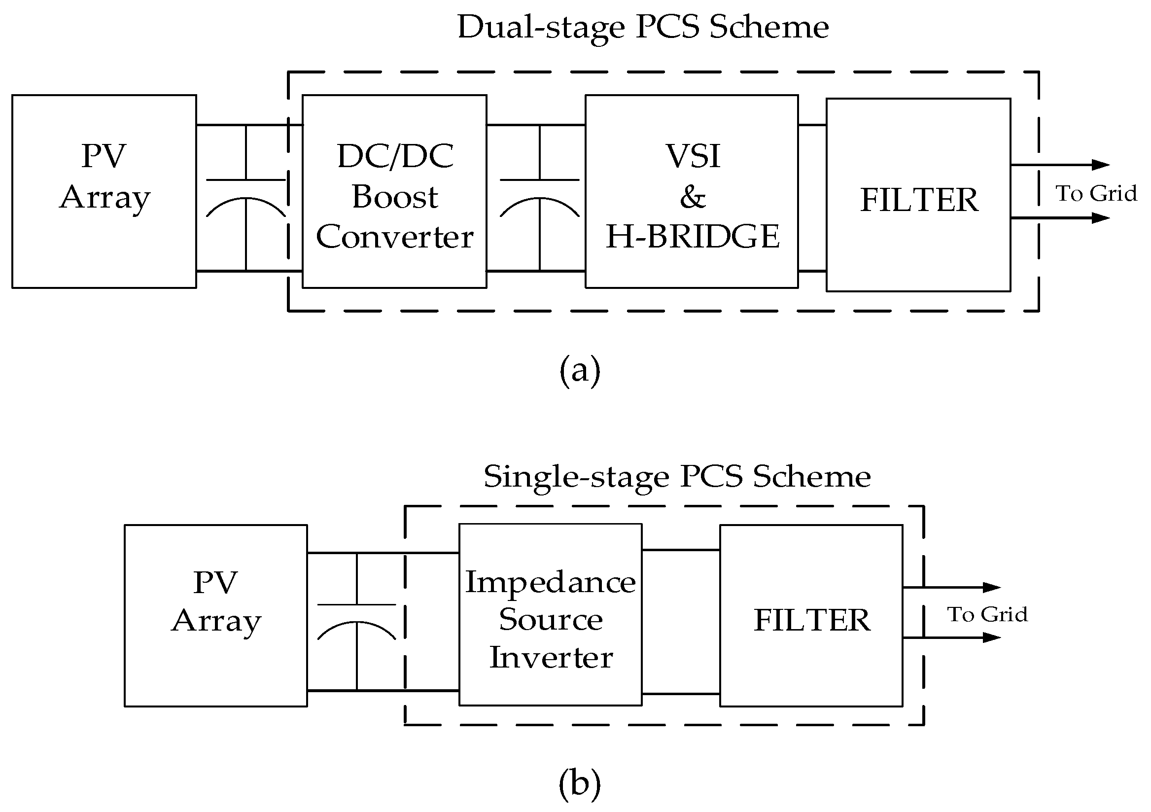
Figure 1 represents the traditional boost converter-based dual-stage and the Z-source inverter (ZSI)-based single-stage PCS. The main function of the PCS is to convert the output DC voltage of the PV unit into 50/60 Hz AC voltage suitable for households and grid applications. Traditionally, a voltage source inverter (VSI) with a DC–DC boost converter comprising the dual-stage PCS is used to convert the DC output power into AC power [7]. This additional DC–DC boost converter increases the size and cost of the PV power generation system. A ZSI for PV systems as presented in [8] obsoletes the additional boost converter with its distinct impedance network. Due to its shoot-through characteristics, the ZSI-based PCS can boost the input voltage of the PV system during voltage fluctuations due to changes in solar irradiation and environmental temperature. Although the ZSI turns the dual-stage traditional system into a single-stage system, it inherits some certain drawbacks regarding its performance, such as limited boost capability, high capacitor voltage stress, and high semiconductor switch voltage stress. For solving these problems, a quasi ZSI (qZSI)-based PCS is proposed in [9] that reduces the high voltage stress of capacitors and satisfactorily suppresses the start-up inrush current of the inverter. Furthermore, the qZSI provides a common ground between the PV input and inverter bridge which minimizes the common mode leakage current problem for PV modules [10]. Although the qZSI improves the performance of traditional ZSI, the boost factor remains similar to that of a ZSI.
For utilizing the full benefit of PV units under different operating conditions, different types of ZSI topologies have been developed for PV applications where the main focus is to improve efficiency. Three new topologies for ZSIs are proposed in [11,12,13], which are named improved ZSI, embedded ZSI, and series ZSI. All these topologies overcome the limitations of the traditional ZSI by lowering the voltage stress and suppressing the inrush current. However, the boost factor remains unaffected, though this is extremely important for PV applications where the output power changes continuously. Furthermore, the lower value of the boost factor significantly reduces the operational efficiency of the PV unit, which is unable to maintain the grid code and the low-voltage ride-through capability. Later efforts have been made to improve the boost factor of existing ZSIs. With this in mind, switched inductor-assisted ZSIs (SL-ZSI) are proposed in [14,15,16,17], while active switch ZSIs are presented in [18,19] to enhance the boost factor. The topologies as presented in [14,15,16,17,18,19] enhance the boost factor as compared to traditional ZSIs and qZSIs. Recently, an enhanced boost ZSI (EB-ZSI) [20], a modified capacitor assisted ZSI (MCA-ZSI) [21], and an embedded switched inductor quasi ZSI (ESL-qZSI) [22] have been used in conjunction with the shoot-through state of the pulse width modulation (PWM) scheme. The topologies in [20,21,22] clearly depict that the boost factor is significantly improved. However, the voltage stresses across the capacitors and semiconductor switches are also increased in these topologies due to the enhancement of the boost factor using the shoot-through state. Furthermore, these topologies do not take care of the common mode leakage current which is generally produced from the PV unit. This leakage current cannot be reduced automatically and, although the double ground feature can be used to overcome this problem, it has not been considered in the literature so far discussed in this paper. This explains the overall size of the PCS and associated cost increase for standalone PV applications due to the requirement of additional transformers. Thus, the size and costs of the ZSI-based PCS is still unable to be reduced.
This paper focuses on the development and performance analysis of a new ZSI topology for a standalone PV system. The main contributions of this paper are as follows:
  • Development of a new ZSI topology for the PCS in applications and topology, termed the switched inductor assisted strong boost Z-source inverter (SL-SBZSI), which includes a series structure impedance network with switched inductor technology.
  • The series structure impedance network is incorporated to reduce the voltage stresses across the capacitors and semiconductor switches compared to all existing topologies.
  • Switched inductor technology is used to enhance the boost factor as compared to other topologies, along with the shoot-through feature.
  • The double ground feature is utilized by incorporating a common ground between the input and output side of the proposed topology to overcome the problem associated with leakage current.
The performance of the proposed scheme is analyzed through both simulation and experimental studies on a simple standalone PV system. The results clearly indicate an improvement in the performance against existing topologies in PV applications.
The remainder of the paper is organized as follows. In Section 2, the operation of the proposed topology is illustrated while Section 3 describes mathematical modeling and characteristics of the proposed topology for analyzing performance against existing topologies. Section 4 includes the simulation results while experimental results are included in Section 5 to analyze the performance of the proposed scheme. Finally, the paper is concluded in Section 6.

2. Operation of Switched Inductor Assisted Strong Boost Z-Source Inverter (SL-SBZSI)

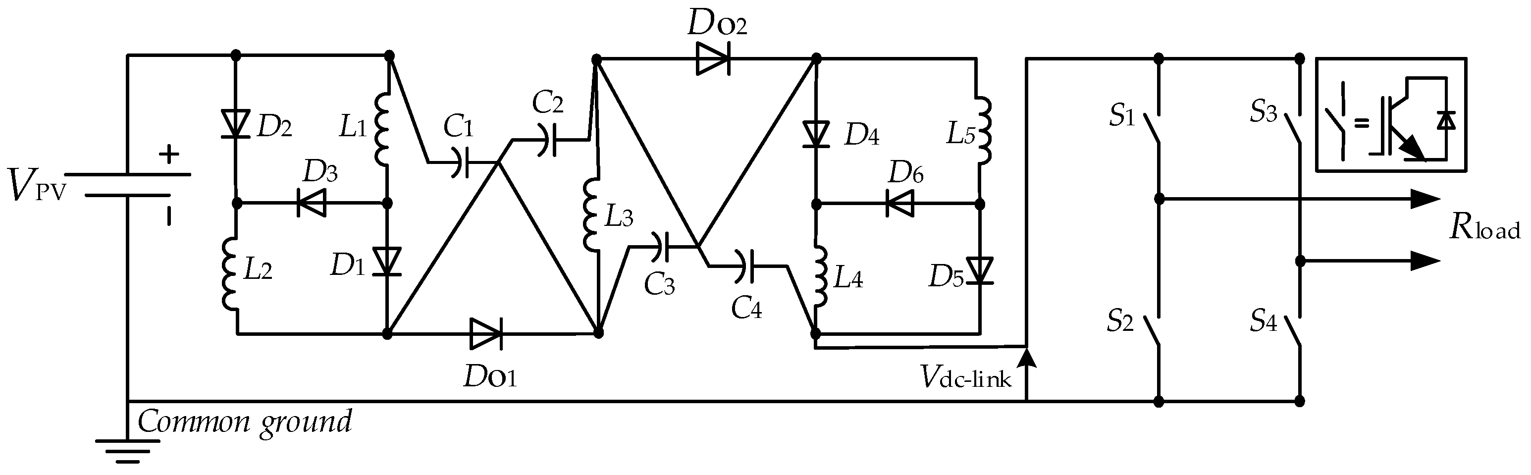
The configuration of the proposed SL-SBZSI is given in Figure 2 where two diode-assisted switched inductor (SL) cells are used. Inductors ( L 1   &   L 2 ) with diodes ( D 1 ,   D 2 ,   &   D 3 ) and inductors ( L 4   &   L 5 ) with diodes ( D 4 , D 5 ,   &   D 6 ) form the left and right sides of switched inductor (SL) cells, respectively. The middle inductor L 3 is commonly merged in the impedance network. This impedance network is placed in series between the PV unit and the input-side of the inverter. The voltages across the capacitors on the both ends of SL cells are equal, i.e., V C 1 = V C 4 , where V C 1 is the voltage across the capacitor, C 1 , and V C 4 is the voltage across the capacitor, C 4 . Similarly, the voltages across the intermediate capacitors are equal, i.e.,   V C 2 = V C 3 , where V C 2 is the voltage across the capacitor, C 2 , and V C 3 is the voltage across the capacitor,   C 3 . 
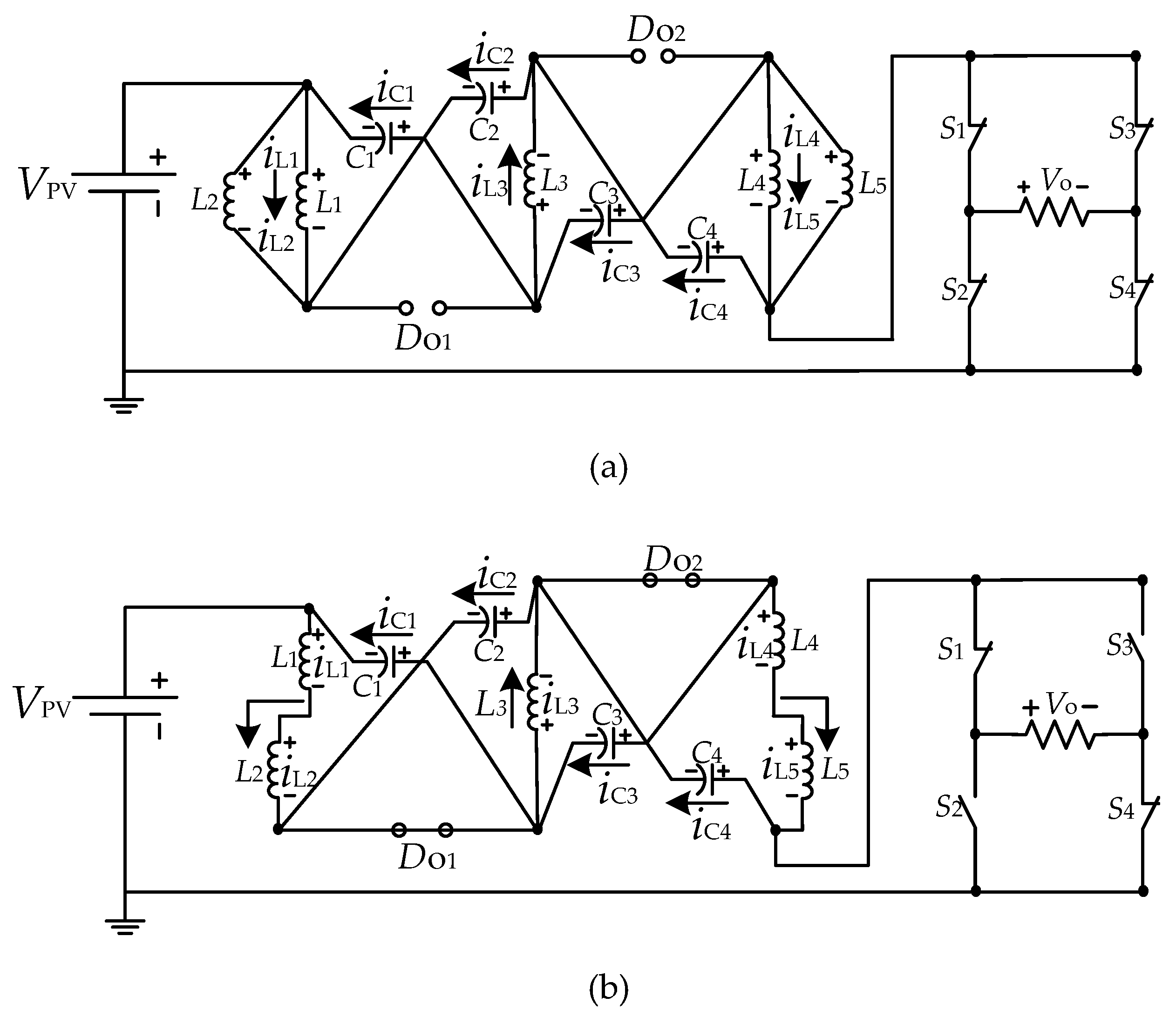
Figure 3 shows the equivalent circuits of the proposed inverter in the shoot-through and normal pulse width modulation (PWM) states, respectively. The operations of both states are explicitly described in the following subsections.

2.1. Shoot-Through State

When there is a voltage sag in the PV energy sources, the shoot-through state enters into the voltage sag mitigation control mode. For this purpose, the normal PWM mode of the proposed inverter turns into the shoot-through mode by gating ON the semiconductor switches   ( S 1 ,   S 2 , S 3 ,   and   S 4 ) of the inverter. During this period, the DC-link voltage V d c l i n k at the input of the inverter becomes zero. The diodes ( D o 1   &   D o 2 ) become reverse-biased while diodes ( D 1 , D 2 , D 4 ,   and   D 5 ) become forward-biased, which makes the SL cells a parallel configuration as shown in Figure 3a. In this operational mode, all inductors L 1 ,    L 2 ,    L 3 ,    L 4 ,   and   L 5 are charged by the capacitors C 1 ,    C 2 ,    C 3 ,   and   C 4 
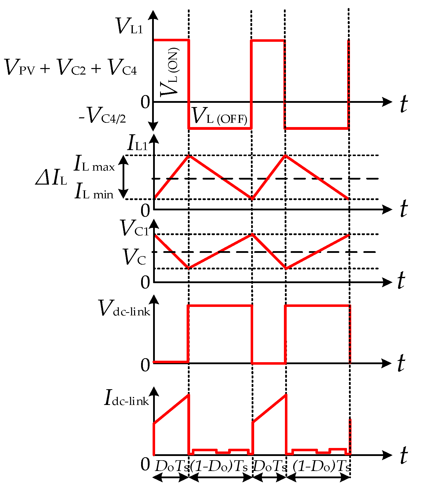
and the inductor currents increase from their minimum to maximum values. The key switching behaviors of inductors and capacitors during the shoot-through mode are depicted in Figure 4. By applying Kirchhoff’s voltage law (KVL) on the shoot-through equivalent circuit, the inductor voltages V L 1   and   V L 3 for inductor    L 1   and   L 3 can be written as follows:
V L 1 = V p v + V C 2 + V C 4   ;        V L 1 = V L 2 = V L 4 = V L 5
V L 3 = 3 (   V p v 2 + V C 2 )
A brief overview of the non-shoot-through state, i.e., the normal PWM state, is provided in the following subsection.

2.2. Non-Shoot-Through/Normal PWM State

When the voltage level of the PV unit remains in the steady-state, the proposed inverter acts like a traditional VSI and during this state, diodes ( D o 1   &   D o 2 ) become forward-biased and diodes ( D 3   &   D 6 ) make the SL cells a series configuration as shown in Figure 3b. During this normal PWM state of the operation, all inductors and the input DC power from the PV unit supply power to the output side of the inverter while all capacitors are being charged. The current through the inductor decreases and, at the same time, the voltage across the capacitor increases. Using KVL on the normal PWM equivalent circuit as shown in Figure 3b, the inductor voltages can be written as follows:
V L 1 = V C 4 2     ;      V L 1 = V L 2 = V L 4 = V L 5
V L 3 = V C 2
Based on these operational states, the factors related to the different characteristics of the proposed SL-SBZSI for standalone PV applications are determined in the following section along with the analysis of these characteristics.

3. Boosting Control Modeling and Characteristics

The steady-state condition is analyzed in this section and the governing mathematical equations of the proposed SL-SBZSI are derived to demonstrate the relationship among different factors, such as the boost factor and duty shoot-through, and the voltage gain and voltage stress across semiconductor switches. The average inductor voltage over one switching period should be zero in order to satisfy the basic volt-sec balance principle for designing power electronics converters. By using the pairs of equations from two different operational modes, i.e., the pairs of Equations (1) and (3) and (2) and (4) and the employing volt-sec principle, the inductor voltages V L 1   and V L 3 can be written as follows:
( V p v + V C 2 + V C 4 )   D o T S + ( V C 4 2   ) ( 1 D o ) T S T s = 0
( 3 V p v 2 + 3 V C 2     )   D o T S +   ( V C 2 )   ( 1 D o ) T s T s   = 0
where D o is the shoot-through duty ratio and T S is the sampling time. By solving Equations (5) and (6), the capacitor voltages V C 4 and V C 2 can be sequentially written as the function of the shoot-through duty ratio and the output voltage of the PV system which can be written as follows:
V C 1 = V C 4 = 2 D o 1 3 D o ( V p v + V C 2 )
V C 2 = V C 3 = 3 D o 2 ( 1 4 D o ) V p v
Substituting Equation (8) into Equation (7), V C 4 can be written as:
V C 1 = V C 4 = D o ( 2 5 D o ) ( 1 7 D o + 12 D o 2 ) V p v
In the non-shoot through mode, the DC-link voltage can be represented as follows:
V d c l i n k = 2 V C 2 + V C 4 + V p v
Therefore, substituting Equations (8) and (9) into Equation (10), it can be written as follows:
V d c l i n k =   ( 2 3 D o 5 D o 2 )   V p v 2 ( 1 7 D o + 12 D o 2 )
The boost factor, B, of the proposed inverter can be written as the ratio of V d c l i n k to   V p v which can be expressed as follows:
B = ( 2 3 D o 5 D o 2 ) 2 ( 1 7 D o + 12 D o 2 )
Again, the relationship between the voltage gain G and modulation index   M of the inverter can be written as:
G = M × B
Using the value of B from Equation (12), the voltage gain in Equation (13) can be written as:
G = M × ( 2 3 D o 5 D o 2 ) 2 ( 1 7 D o + 12 D o 2 )
In the proposed SL-SBZSI topology, the simple boost control (SBC) PWM method as presented in [23] is adopted in order to demonstrate the operation of the inverter control system. Other traditional control techniques can be found in [24,25,26,27] for the shoot-through scheme of ZSIs. In the SBC control method, two modulation signals with 180 0 
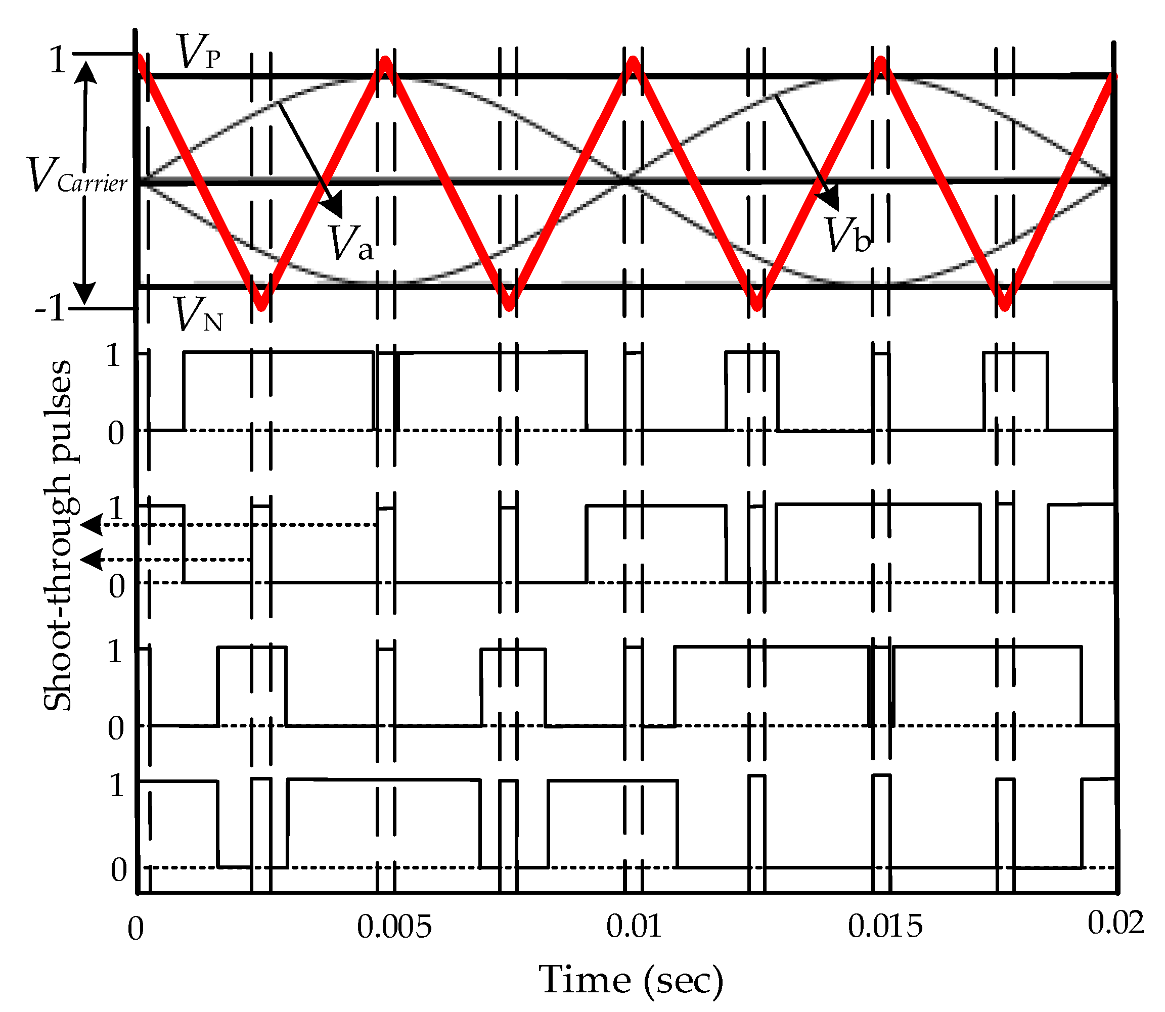
phase shift are compared with a high frequency triangular carrier signal for generating the PWM switching signals. For the generation of the shoot-through pulses during the zero-state operation of the inverter, two constant positive and negative voltages are also used and compared with the triangular carrier signal. The shoot-through pulses are generated when the carrier signal is greater or lower than these constant positive and negative voltages. The generation of switching pulses for the proposed SL-SBZSI using the shoot-through scheme is shown in Figure 5, for which the relationship between the shoot-through duty ratio D o and modulation index M   can be written as:
D o = 1 M
and:
M = 1 D o
By substituting Equation (16) into Equation (14), the voltage gain of the inverter can be written as follows:
G = ( 1 D o   ) ( 2 3 D o 5 D o 2 )     2 ( 1 7 D o + 12 D o 2 )
The governing equations, representing the relationship among different factors for the proposed topology by considering solar PV applications are summarized in Table 1.
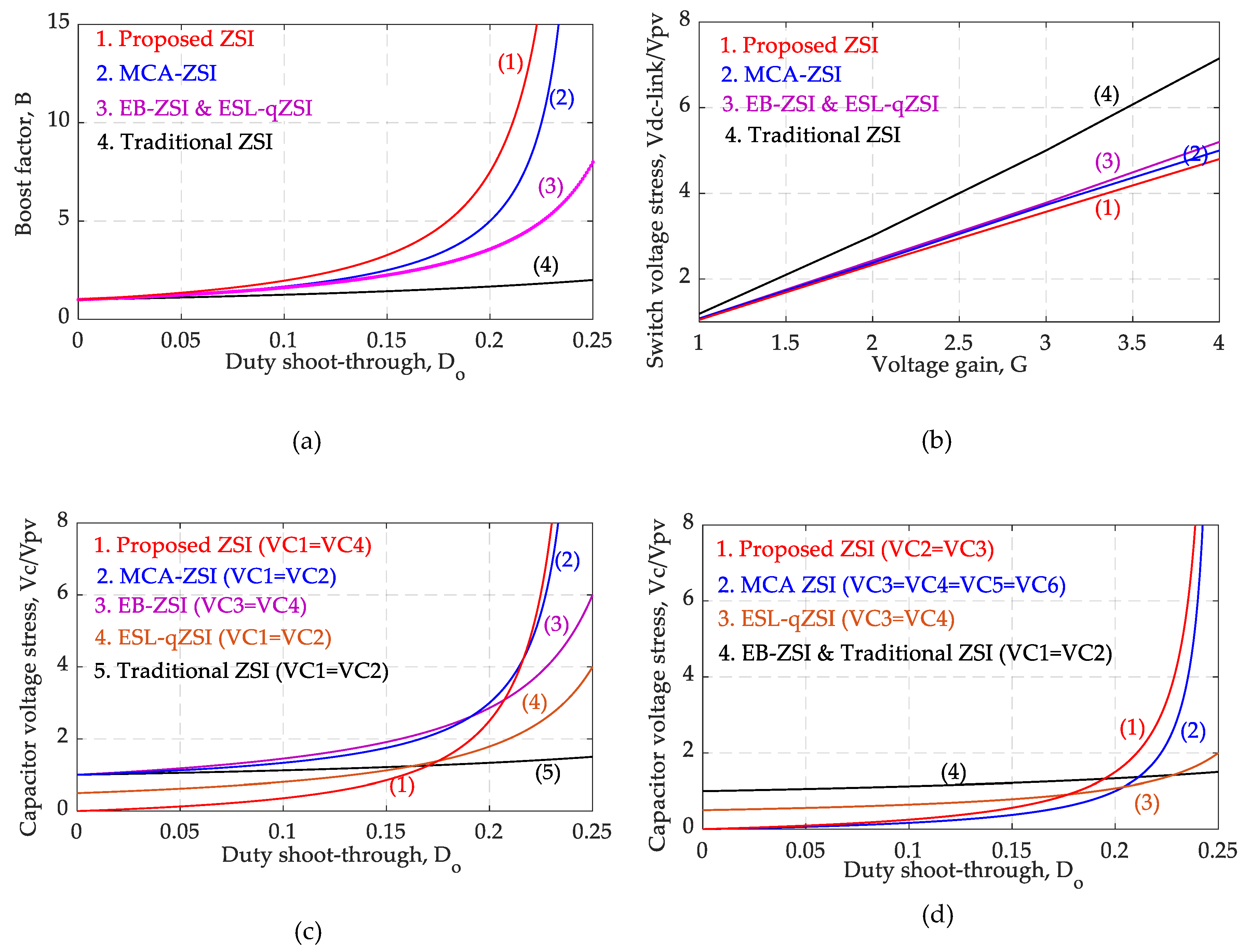
The characteristic curves of the proposed inverter, along with three switched inductor/capacitor assisted ZSI topologies, namely, MCA-ZSI, EB-ZSI, and ESL-qZSI, and traditional ZSI are given in Figure 6. The comparisons are made based on boost factor, inverter switch voltage stress, and capacitor voltage stress (for both low- and high-stages). Figure 6a clearly shows that the proposed topology has better boosting capability compared to other existing topologies. At the same time, the switch voltage stress of the proposed topology is lower than other topologies, i.e., the switches in the proposed ZSI experience less voltage stresses, which can easily be seen from Figure 6b. The capacitor voltage stress during the high stage is moderate with the proposed topology as depicted in Figure 6c. However, during the low stage, the proposed topology allows the capacitors to handle more voltage stresses as compared to other topologies up to an acceptable duty shoot-through which is evident from Figure 6d. By considering all these factors, it can easily be seen that the proposed topology provides better performance compared to recently developed similar topologies for almost all cases, although the performance of the proposed topology is moderate for handling the capacitor voltage during the high stage. However, this stage is a very unusual situation, as the maximum rated voltage is considered during the selection of the capacitor, and such a situation does not appear for PV applications. Hence, the proposed topology will improve the performance for any application, including standalone PV applications. The performance of the proposed SL-SBZSI is analyzed in the following sections through both simulation and experimental results.

4. Simulation Results and Discussions

In this section, the improved performance of the proposed topology is verified through simulation results in MATLAB/Simulink. Simulation studies are carried out on a typical standalone PV system with the designed SL-SBZSI as shown in Figure 2. The parameters used for these simulations are provided in Table 2. In this paper, two different case studies are performed and one of these two cases considers solar irradiation as constant with varying temperature while the other case is used to demonstrate the performance by considering constant temperature but varying solar irradiation. These two cases are mainly considered to demonstrate the shoot-through and normal operations of the designed PCS. Finally, the performance of the proposed inverter is also analyzed for a dynamic condition in order to demonstrate its voltage compensation behaviors.

4.1. Case-1: Shoot-Through State: Constant Solar Irradiation at 1000   W / m 2 but Varying Temperature from 25   ° C to 55   ° C

The output power of the PV unit changes with temperature even if solar irradiation is constant. During standard operating conditions, solar irradiation is generally considered to be 1000   W / m 2 , while the temperature is 25   ° C . In this case study, the standard value of solar irradiation is considered and the temperature is varied from 25   ° C to 55   ° C   , which corresponds to an output voltage of the PV unit as 116.6   V , i.e., V p v = 116.6   V . In this case, the AC load voltage is attained as 78.38   V   ( rms ) which is achieved by maintaining the modulation index, M = 0.8   and the shoot-through duty ratio, D o = 0.03 . From the simulation result as shown in Figure 7a, the DC-link voltage is 138.56   V   for which the boost factor becomes 1.188 , i.e.,   B = 1.188   , and the calculated value of this boost factor using Equation (12) is 1.189. At this instant, the inverter voltage gain ( G ) becomes 1.154 , which can easily be calculated using Equation (17), and the capacitor voltages can be calculated from Equations (8) and (9). The calculated values of these voltages are V C 1 = V C 4 = 8.08   V and V C 2 = V C 3 = 5.96   V . From the simulation result in Figure 7a, it can be seen that these capacitor voltages match with their corresponding calculated values. The output load voltage is shown in Figure 7b, from where it can be observed that the peak voltage of the load is 110.84   V , which corresponds to the rms value of 78.38   V . Thus, it can be said that the simulation result closely matches with the analytical result and the designed SL-SBZSI ensures the desired operational performance with changes in temperature.
From the results and analyses in Section 3, it is clearly noticeable that the boost factor of the proposed topology increased nearly 1.048 times compared to the conventional MCA-ZSI, EB-ZSI and ESL-qZSI topologies for the shoot-through duty ratio of D 0 = 0.03 . The voltage stress across the high-stage capacitors is around 0.069 times the applied input voltage, whereas conventional MCA-ZSI, EB-ZSI, and ESL-qZSI have stresses of 1.0682 , 1.1364 ,   and   1.0682 times, respectively. On the other hand, the MCA-ZSI reduces the stress to the value of 0.034 for the low-stage capacitor which is 0.667 times lower than the proposed SL-SBZSI topology. However, for EB-ZSI and ESL-qZSI, the values are 1.0670 and 0.533 times the input voltage, respectively. Further gain can be achieved fairly by increasing the duty ratio according to the characteristic curves as shown in Figure 6a. From the characteristic curves as presented in Figure 6, it can be said that the proposed topology for the PV application improves the overall behavior in terms of different factors, such as the inverter gain, voltage stress across capacitors, and semiconductor switch voltage stress, compared to conventional topologies.

4.2. Case-2: Normal PWM State/Non-Shoot-Through State: Varying Irradiation from 250   W / m 2 to 1000   W / m 2 but Constant Temperature at   25   ° C

The changes in solar irradiance decrease the output current and power while maintaining the sufficient voltage level. For the extraction of the maximum power from the PV unit, the output voltage of the PV unit is 146.5   V at the constant temperature of 25   ° C . For this case study, the designed SL-SBZSI inverter works with its normal PWM mode where it is not essential to boost the voltage and, thus, the shoot-through duty ratio and modulation index are kept   D o = 0.00 and M = 0.8 , respectively. In this situation, the voltages across capacitors will be zero according to Equations (8) and (9) as   D o = 0 , which can also be seen from Figure 8a. There are some slight variations across capacitors, although these values are not far away from zero.
Figure 8b clearly depicts that the peak value of the load voltage is 117.2   V for which the corresponding rms value is 82.8   V . Thus, it can be said that the designed ZSI also ensures the desired performance with the change in the solar irradiation.

4.3. Dynamic Voltage Compensation Behaviors of the Proposed SL-SBZSI

For this condition, the simulation is conducted for a total time period of   0.6   s . From Figure 9a, it can be noticed that the inverter operates in normal PWM state at t = ( 0.0     0.2 )   s , in voltage sag state at     t   = ( 0.2     0.4 )   s , and again the normal PWM state is retained at    t   = ( 0.4     0.6 )   s . The corresponding load voltage is shown in Figure 9b. At t = ( 0.2     0.4 )   s , the designed SL-SBZSI boosts the load voltage for compensating the voltage sag by injecting boost voltage as shown in Figure 9c and the boosted output load voltage is retained to the desired level as shown in Figure 9d.
This operation of the designed SL-SBZSI is summarized in Table 3 where the inverter operates at the shoot-through state from   t   = ( 0.4     0.6 )   s . From Figure 10, the operation states are segregated and shown in the same window from the normal PWM to the shoot-through state.
At first, the voltage sag is detected at t = 0.2   s and the input voltage is found to be   V p v = 116.6   V . During this time, the shoot-through duty ratio is kept as D o = 0.00   and the output load voltage becomes 65.9   V   ( rms ) ,   which is less than the desired voltage. At time   t   = 0.4    s , the shoot-through duty ratio D o = 0.03 is applied until t = 0.6   s .   Hence, the designed SL-SBZSI starts the boosting effect and satisfactorily retains the standard load voltage level, i.e., V l o a d = 78.38   V   ( rms ) . The corresponding output load current is also shown in Figure 10 where this value is 1.27   A , i.e.,   I l o a d = 1.27   A   ( rms ) . Hence, the designed SL-SBZSI exhibits dynamic voltage compensation characteristics.

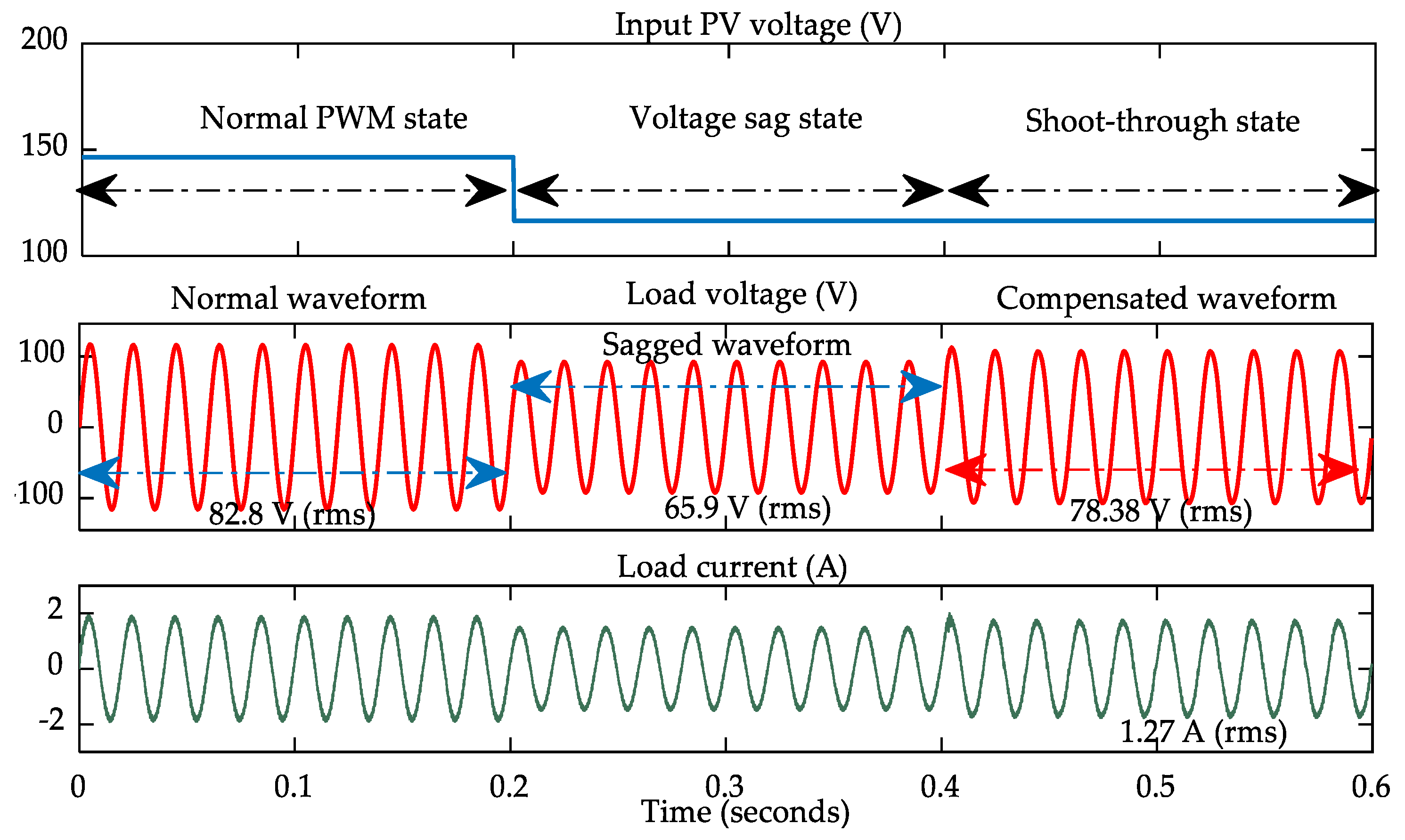
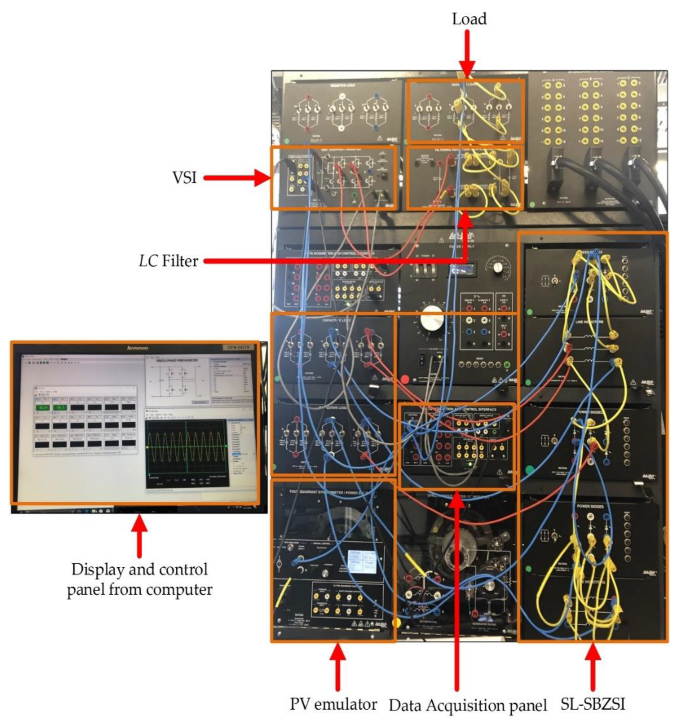
5. Experimental Validation

The experimental setup for evaluating the performance of the proposed topology is shown in Figure 11, from where it can be seen that a PV emulator is connected to a VSI through the proposed topology. At the output of the inverter an LC filter is used and, finally, the power is delivered to a resistive load. The parameters used for this system are listed in Table 4.
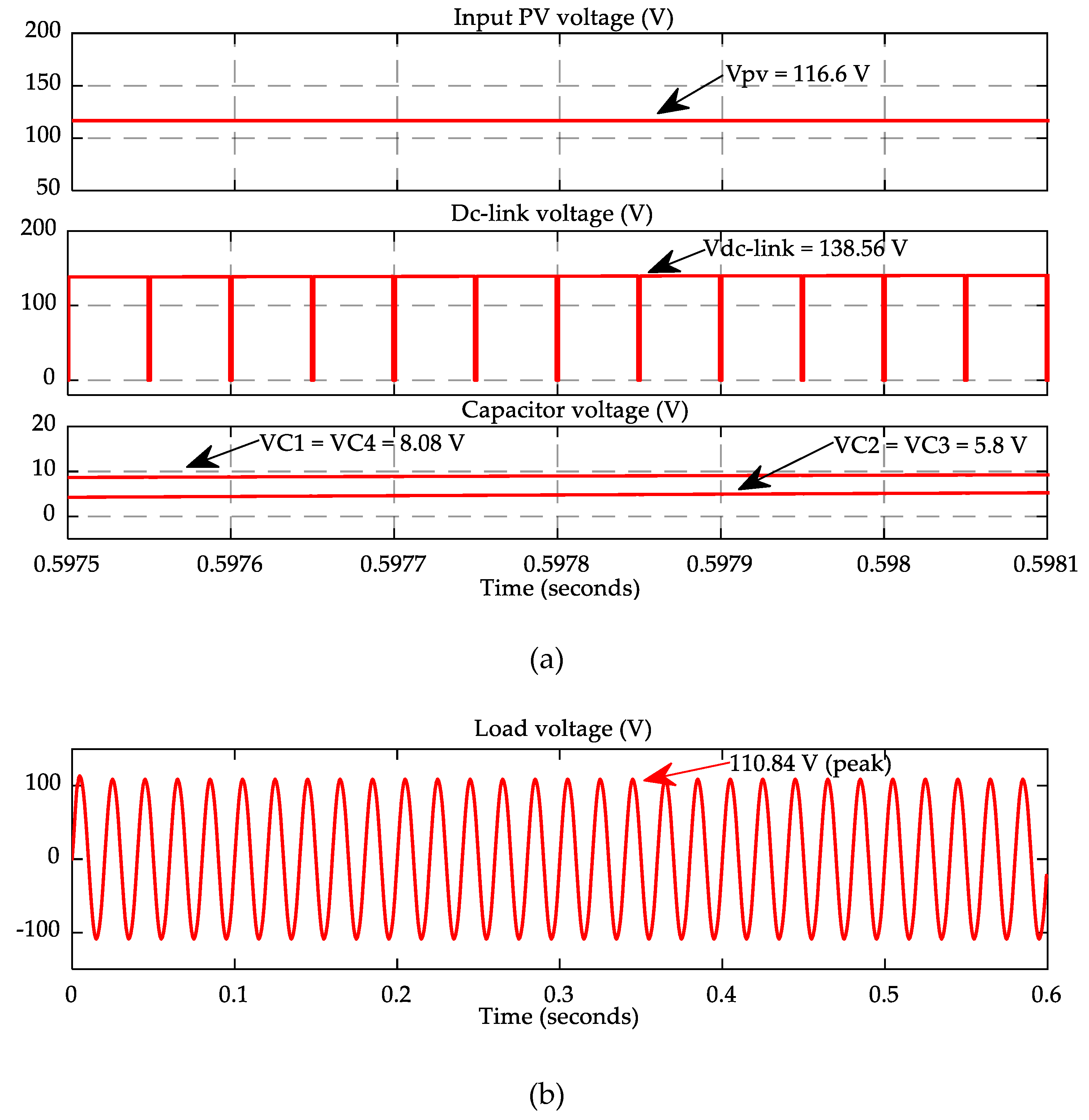
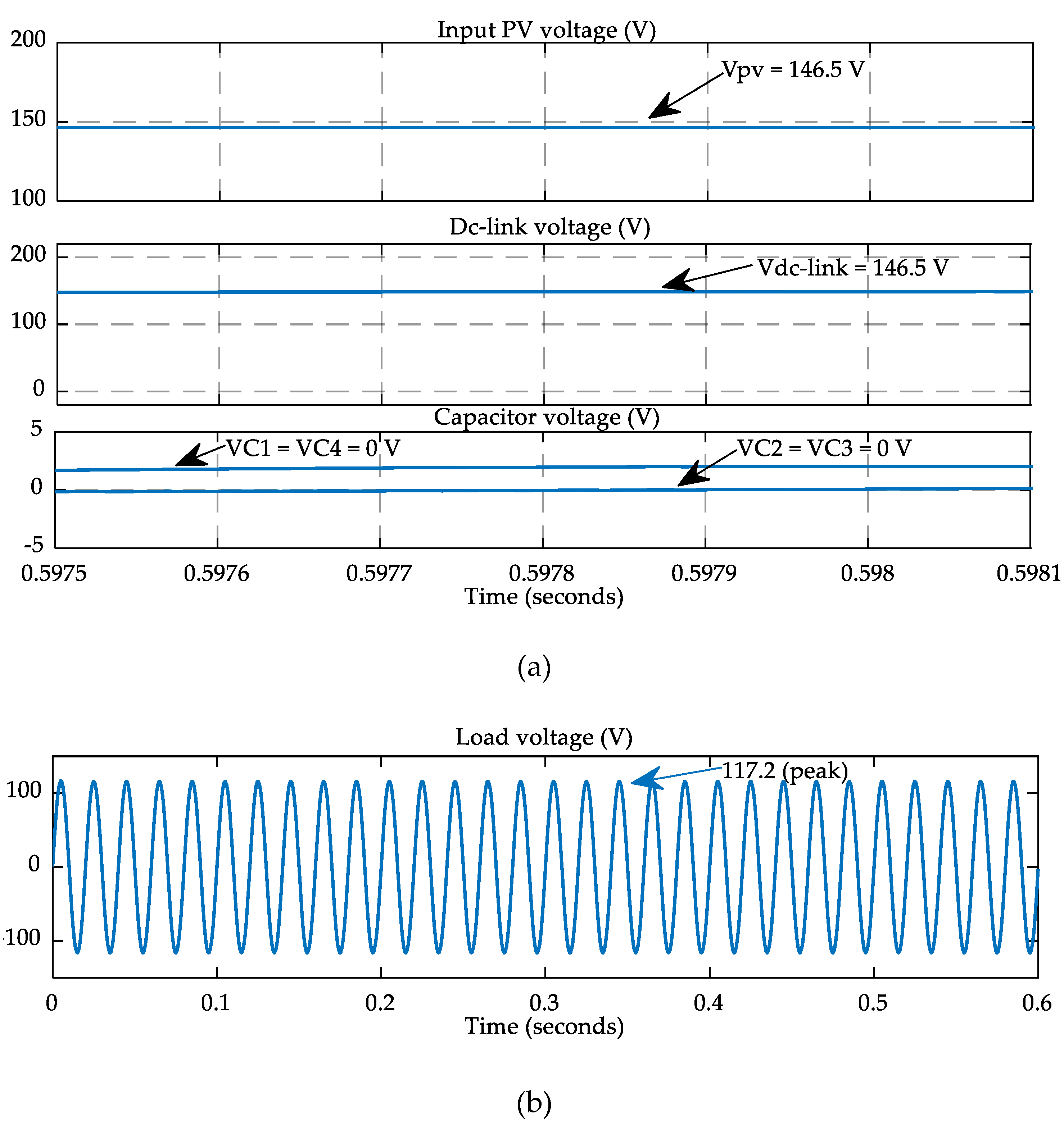
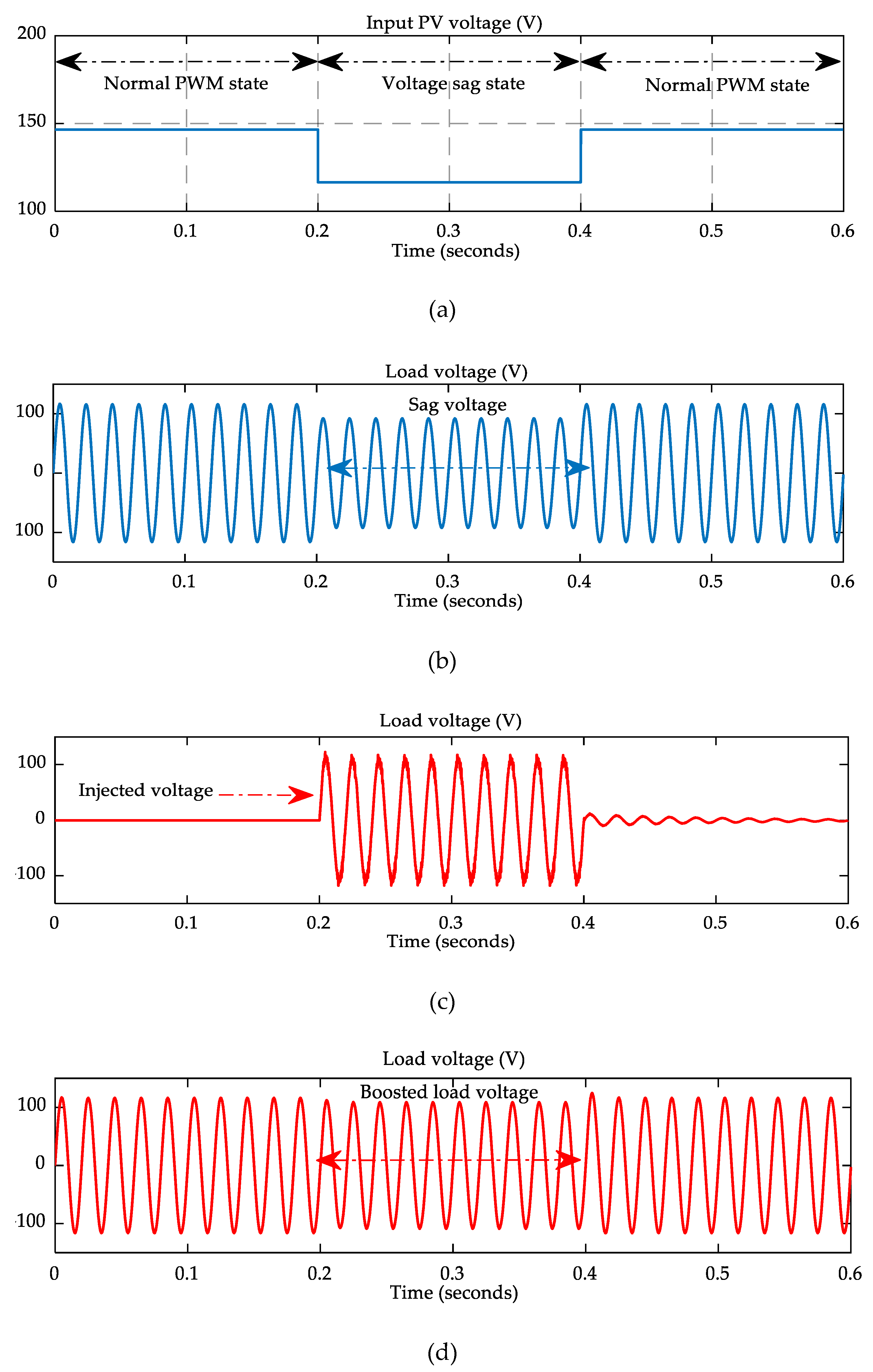
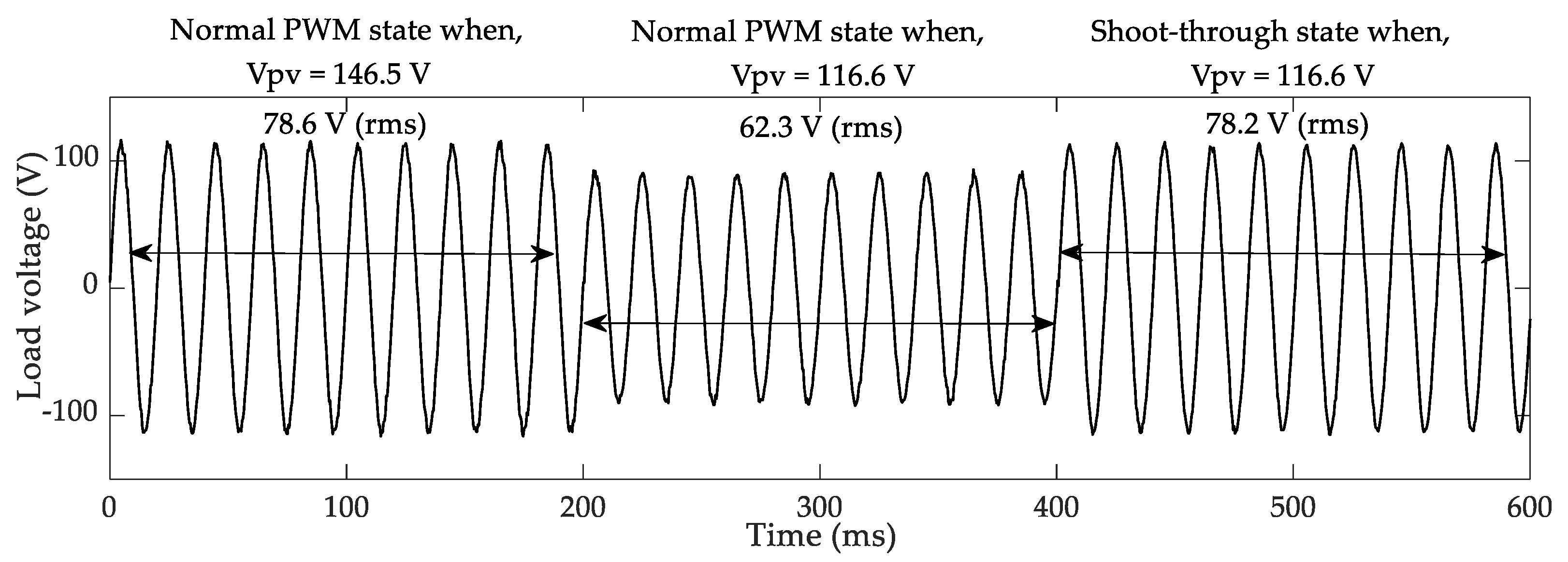
During the experimental study, the performance of the proposed topology for the standalone PV application is analyzed to ensure its ability for the dynamic voltage compensation on a practical system. The experiment is conducted by considering the modulation index as M = 0.8   and duty ratio of shoot-through D o = 0.03 , and the standalone PV system is operated using the normal PWM scheme until t = 200   ms . At this stage, the input PV voltage is 146.5   V and the corresponding load voltage is 78.6   V   ( rms ) , as shown in Figure 12. However, the input voltage drops to 116.6   V due to changes in the PV unit and, at this stage, the experimental system is operated until t = 400   ms where the normal PWM scheme is still used to generate the switching pulses for the VSI. In this condition, the system will experience voltage sag, which can also be seen from Figure 12, and here the rms value of the load voltage is 62.3   V . However, this voltage sag can be compensated by incorporating a shoot-through PWM scheme while keeping the input PV voltage at the same level, i.e., at 116.6   V , and this is applied at t = 400   ms . Now, the system is operated until t = 600   ms and, from Figure 12, it can be seen that the load voltage settles down to 78.2   V   ( rms ) ,   which is close to the initial load voltage. However, slight notches in the output voltage waveforms are noticeable in the experimental results. The notches or, in other words, the spurious harmonic effect in the output load voltage, is caused by the modulation control algorithm of the Z-source inverter, which generates switching noise for semiconductor devices and, consequently, distorts the output load voltage of the proposed inverter. The space vector pulse width modulation (SVPWM) technique can be employed to reduce this spurious harmonic effect, as SVPWM has a reduced commutation time in semiconductor switches, which ultimately reduces the harmonic content in the inverter output voltage. Moreover, the performance of the designed SL-SBZSI is consistent in both simulation and experimental results.

6. Conclusions

This paper presented a novel ZSI for standalone PV power conditioning systems. The designed ZSI has a strong boosting capability over a wide range of boost factors with respect to the low shoot-through duty ratio. During mitigation of the voltage sag, this topology significantly reduces the capacitor voltage stress and inverter switch voltage stress compared to conventional ZSIs, which guarantees a cost reduction factor for a single-stage PCS. With the combination of all existing features of traditional ZSIs, the designed SL-SBZSI adds an additional double ground that promises better performance for the PV system. The simulation results for both shoot-through and normal PWM states clearly demonstrate the effectiveness of the proposed topology, and the results of dynamic behavior for voltage compensation show the smooth operation of the designed SL-SBZSI-based PCS for transferring power from the PV unit to loads in a standalone system during the voltage sag condition. Experimental results associated with the dynamic voltage compensation also exhibit similar patterns to that of the simulation results. From simulation results, it is also identified that the proposed topology provides moderate performance in terms of handling the capacitor voltage stresses during the high-stage. Future work will deal with the reduction of this voltage stress for both grid-connected and standalone PV applications.

Author Contributions

Conceptualization, N.S.; Formal analysis, N.S. and M.A.M.; Funding acquisition, R.K. and M.A.M.; Investigation, N.S.; Methodology, N.S.; Project administration, R.K. and M.F.R.; Software, N.S.; Supervision, R.K., M.A.M. and M.F.R.; Validation, N.S. and M.A.M.; Writing—original draft, N.S.; Writing—review & editing, M.A.M.

Funding

The work was supported by the Graduate Assistantship (GA) scheme of Universiti Teknologi PETRONAS (UTP).

Acknowledgments

The authors would like to thank Dr. Tushar Kanti Roy from Electrical Power & Energy Systems Research Lab (EPESRL) at Deakin University, Australia for his effort to conduct the experiment.

Conflicts of Interest

The authors declare no conflicts of interest.

References

  1. Chauhan, A.; Saini, R. A review on Integrated Renewable Energy System based power generation for stand-alone applications: Configurations, storage options, sizing methodologies and control. Renew. Sustain. Energy Rev. 2014, 38, 99–120. [Google Scholar] [CrossRef]
  2. Genc, R.; Alas, M.O.; Harputlu, E.; Repp, S.; Kremer, N.; Castellano, M.; Colak, S.G.; Ocakoglu, K.; Erdem, E. High-Capacitance Hybrid Supercapacitor Based on Multi-Colored Fluorescent Carbon-Dots. Sci. Rep. 2017, 7, 11222. [Google Scholar] [CrossRef] [PubMed]
  3. Repp, S.; Harputlu, E.; Gurgen, S.; Castellano, M.; Kremer, N.; Pompe, N.; Wörner, J.; Hoffmann, A.; Thomann, R.; Emen, F.M.; et al. Synergetic effects of Fe 3+ doped spinel Li 4 Ti 5 O 12 nanoparticles on reduced graphene oxide for high surface electrode hybrid supercapacitors. Nanoscale 2018, 10, 1877–1884. [Google Scholar] [CrossRef] [PubMed]
  4. Himanshu;Rao, S.S.; Punnoose, D.; Sathishkumar, P.; Gopi, C.V.V.M.; Bandari, N.; Durga, I.K.; Krishna, T.N.V.; Kim, H.-J. Development of Novel and Ultra-High-Performance Supercapacitor Based on a Four Layered Unique Structure. Electronics 2018, 7, 121. [Google Scholar] [CrossRef]
  5. Huffstutler, J.D.; Wasala, M.; Richie, J.; Barron, J.; Winchester, A.; Ghosh, S.; Yang, C.; Xu, W.; Song, L.; Kar, S.; et al. High Performance Graphene-Based Electrochemical Double Layer Capacitors Using 1-Butyl-1-methylpyrrolidinium tris (pentafluoroethyl) trifluorophosphate Ionic Liquid as an Electrolyte. Electronics 2018, 7, 229. [Google Scholar] [CrossRef]
  6. International Energy Outlook 2016. [Online]. Available online: https://www.eia.gov/outlooks/ieo/pdf/0484(2016).pdf (accessed on 10 October 2018).
  7. Meneses, D.; Blaabjerg, F.; García, Ó.; Cobos, J.A. Review and Comparison of Step-Up Transformerless Topologies for Photovoltaic AC-Module Application. IEEE Trans. Power Electron. 2013, 28, 2649–2663. [Google Scholar] [CrossRef] [Green Version]
  8. Huang, Y.; Shen, M.; Peng, F.Z.; Wang, J. $Z$-Source Inverter for Residential Photovoltaic Systems. IEEE Trans. Power Electron. 2006, 21, 1776–1782. [Google Scholar] [CrossRef]
  9. Ge, B.; Abu-Rub, H.; Peng, F.Z.; Lei, Q.; De Almeida, A.T.; Ferreira, F.J.T.E.; Sun, D.; Liu, Y. An Energy-Stored Quasi-Z-Source Inverter for Application to Photovoltaic Power System. IEEE Trans. Ind. Electron. 2013, 60, 4468–4481. [Google Scholar] [CrossRef]
  10. Yang, B.; Li, W.; Gu, Y.; Cui, W.; He, X. Improved Transformerless Inverter With Common-Mode Leakage Current Elimination for a Photovoltaic Grid-Connected Power System. IEEE Trans. Power Electron. 2012, 27, 752–762. [Google Scholar] [CrossRef]
  11. Tang, Y.; Xie, S.; Zhang, C.; Xu, Z. Improved Z-source inverter with reduced Z-source capacitor voltage stress and soft-start capability. IEEE Trans. Power Electron. 2009, 24, 409–415. [Google Scholar] [CrossRef]
  12. Loh, P.C.; Gao, F.; Blaabjerg, F. Embedded EZ-source inverters. IEEE Trans. Ind. Appl. 2010, 46, 256–267. [Google Scholar]
  13. Tang, Y.; Wei, J.; Xie, S. Grid-tied photovoltaic system with series Z-source inverter. IET Renew. Power Gen. 2013, 7, 275–283. [Google Scholar] [CrossRef]
  14. Zhu, M.; Yu, K.; Luo, F.L. Switched Inductor Z-Source Inverter. IEEE Trans. Power Electron. 2010, 25, 2150–2158. [Google Scholar]
  15. Nguyen, M.-K.; Lim, Y.-C.; Cho, G.-B. Switched-inductor quasi-Z-source inverter. IEEE Trans. Power Electron. 2011, 26, 3183–3191. [Google Scholar] [CrossRef]
  16. Nguyen, M.-K.; Lim, Y.-C.; Choi, J.-H. Two switched-inductor quasi-Z-source inverters. IET Power Electron. 2012, 5, 1017–1025. [Google Scholar] [CrossRef]
  17. Deng, K.; Zheng, J.; Mei, J. Novel switched-inductor quasi-Z-source inverter. J. Power Electron. 2014, 14, 11–21. [Google Scholar] [CrossRef]
  18. Ho, A.-V.; Chun, T.-W.; Kim, H.-G. Extended boost active-switched-capacitor/switched-inductor quasi-Z-source inverters. IEEE Trans. Power Electron. 2015, 30, 5681–5690. [Google Scholar] [CrossRef]
  19. Babaei, E.; Asl, E.S.; Babayi, M.H.; Laali, S. Developed embedded switched-Z-source inverter. IET Power Electron. 2016, 9, 1828–1841. [Google Scholar] [CrossRef]
  20. Fathi, H.; Madadi, H. Enhanced-boost Z-source inverters with switched Z-impedance. IEEE Trans. Ind. Electron. 2016, 63, 691–703. [Google Scholar] [CrossRef]
  21. Ho, A.-V.; Chun, T.-W. Modified Capacitor-Assisted Z-Source Inverter Topology with Enhanced Boost Ability. J. Power Electron. 2017, 17, 1195–1202. [Google Scholar]
  22. Abbasi, M.; Eslahchi, A.H.; Mardaneh, M. Two Symmetric Extended-Boost Embedded Switched-Inductor Quasi-Z-Source Inverter with Reduced Ripple Continuous Input Current. IEEE Trans. Ind. Electron. 2018, 65, 5096–5104. [Google Scholar] [CrossRef]
  23. Pham, C.-T.; Shen, A.; Dzung, P.Q.; Anh, N.B.; Phu, N.X. A comparison of control methods for Z-source inverter. Energy Power Eng. 2012, 4, 187. [Google Scholar] [CrossRef]
  24. Shen, M.; Wang, J.; Joseph, A.; Peng, F.Z.; Tolbert, L.M.; Adams, D.J. Maximum constant boost control of the Z-source inverter. In Proceedings of the 39th IAS Annual Meeting Conference Record of the 2004 IEEE Industry Applications Conference, Seattle, WA, USA, 3–7 October 2004; Volume 1. [Google Scholar]
  25. Peng, F.Z.; Shen, M.; Qian, Z. Maximum boost control of the Z-source inverter. IEEE Trans. Power Electron. 2005, 20, 833–838. [Google Scholar] [CrossRef]
  26. Shen, M.; Wang, J.; Joseph, A.; Peng, F.Z.; Tolbert, L.M.; Adams, D.J. Constant boost control of the Z-source inverter to minimize current ripple and voltage stress. IEEE Trans. Ind. Appl. 2006, 42, 770–778. [Google Scholar] [CrossRef]
  27. Ali, U.S.; Kamaraj, V. A novel space vector PWM for Z-source inverter. In Proceedings of the 2011 1st International Conference on Electrical Energy Systems, Newport Beach, CA, USA, 3–5 January 2011; pp. 82–85. [Google Scholar]
Figure 1. Photovoltaic (PV) power conditioning scheme: (a) traditional dual stage conversion and (b) Z-source inverter (ZSI) based single-stage conversion.
Electronics 08 00139 g001
Figure 2. Proposed switched inductor assisted strong boost Z-source inverter (SL-SBZSI).
Electronics 08 00139 g002
Figure 3. Equivalent circuits of the SL-SBZSI: (a) shoot-through state and (b) normal pulse width modulation (PWM) state.
Electronics 08 00139 g003
Figure 4. Key switching waveforms for the SL-SBZSI.
Electronics 08 00139 g004
Figure 5. Shoot-through control signal waveforms for the SL-SBZSI.
Electronics 08 00139 g005
Figure 6. Characteristic curves of the SL-SBZSI: (a) duty ratio vs boost factor, (b) voltage gain vs switch voltage stress, (c) duty ratio vs capacitor voltage stress (high-stage), and (d) duty ratio vs capacitor voltage stress (low-stage).
Electronics 08 00139 g006
Figure 7. Simulation results during shoot-through state: (a) output voltage of the PV unit, DC-link voltage, and capacitor voltages, and (b) output load voltage.
Electronics 08 00139 g007
Figure 8. Simulation results during normal PWM state: (a) output voltage of the PV unit, DC-link voltage, and capacitor voltages; and (b) output load voltage.
Electronics 08 00139 g008
Figure 9. Simulation results: (a) output voltage of the PV unit, (b) sagged load voltage, (c) injected shoot-through voltage to load, and (d) output boosted load voltage.
Electronics 08 00139 g009
Figure 10. Simulation results during the dynamic condition.
Electronics 08 00139 g010
Figure 11. Experimental setup.
Electronics 08 00139 g011
Figure 12. Experimental result for the dynamic voltage compensation.
Electronics 08 00139 g012
Table 1. Governing equations of SL-SBZSI.
No.ParametersEquations
1Boost factor, B ( 2 3 D o 5 D o 2 ) 2 ( 1 7 D o + 12 D o 2 )
2DC-link voltage, V d c l i n k ( 2 3 D o 5 D o 2 )   2 ( 1 7 D o + 12 D o 2 ) V p v
3Capacitor voltage, V C     V C 2 = V C 3 =   3 D o 2 ( 1 4 D o ) V p v
V C 1 = V C 4 =   D o ( 2 5 D o ) ( 1 7 D o + 12 D o 2 ) V p v
4Voltage gain, G ( 1 D o ) ( 2 3 D o 5 D o 2 ) 2 ( 1 7 D o + 12 D o 2 )
Table 2. Simulation parameters for the SL-SBZSI.
No.ParametersSymbolsValue
1Z-source impedance network: Inductor L 1 = L 2 = L 3 = L 4 = L 5 700   μ H
2Z-source impedance network: Capacitor C 1 = C 2 = C 3 = C 4 500   μ F
3Switching frequency f S 10   kHz
4Output filter: Inductor L f 1.2   mH
5Output filter: Capacitor C f 10   μ F
6Load Resistance R l o a d 65  
Table 3. Dynamic operation states.
No.Output Voltage of the PV UnitShoot-Through Duty CycleOperation PeriodLoad VoltageInverter Mode
1 146.5   V D o = 0.00 t   = ( 0.0     0.2 )   s 82.8   V ( rms ) Normal PWM
2 116.6   V D o = 0.00 t   = ( 0.2     0.4 )   s 65.9   V ( rms ) Normal PWM
3 116.6   V D o = 0.03 t   = ( 0.4     0.6 )   s 78.38   V ( rms ) Shoot-through
Table 4. Experimental parameters.
No.ParametersSymbolsValue
1Z-source impedance network: Inductor L 1 = L 2 = L 3 = L 4 = L 5 25   mH
2Z-source impedance network: Capacitor C 1 = C 2 = C 3 = C 4 0.66   µ F
3Switching frequency f S 10   kHz
4Output filter: Inductor L f 8   mH
5Output filter: Capacitor C f 6.5   μ F
6Load Resistance R l o a d 342.86  

